AN3216 Debug management
Doc ID 17496 Rev 5 21/30
5.3.1 SWJ debug port pins
Five pins are used as outputs for the SWJ-DP as alternate functions of general-purpose
I/Os (GPIOs). These pins, shown in Tabl e 2, are available on all packages.
5.3.2 Flexible SWJ-DP pin assignment
After reset (SYSRESETn or PORESETn), all five pins used for the SWJ-DP are assigned as
dedicated pins which are immediately usable by the debugger host (note that the trace
outputs are not assigned except if explicitly programmed by the debugger host).
However, the STM32L1xxx MCU implements a register to disable all or part of the SWJ-DP
port, and so releases the associated pins for general-purpose I/O usage. This register is
mapped on an APB bridge connected to the Cortex™-M3 system bus. It is programmed by
the user software program and not by the debugger host.
Table 3 shows the different possibilities for releasing some pins.
For more details, see the STM32L15xx reference manual (RM0038).
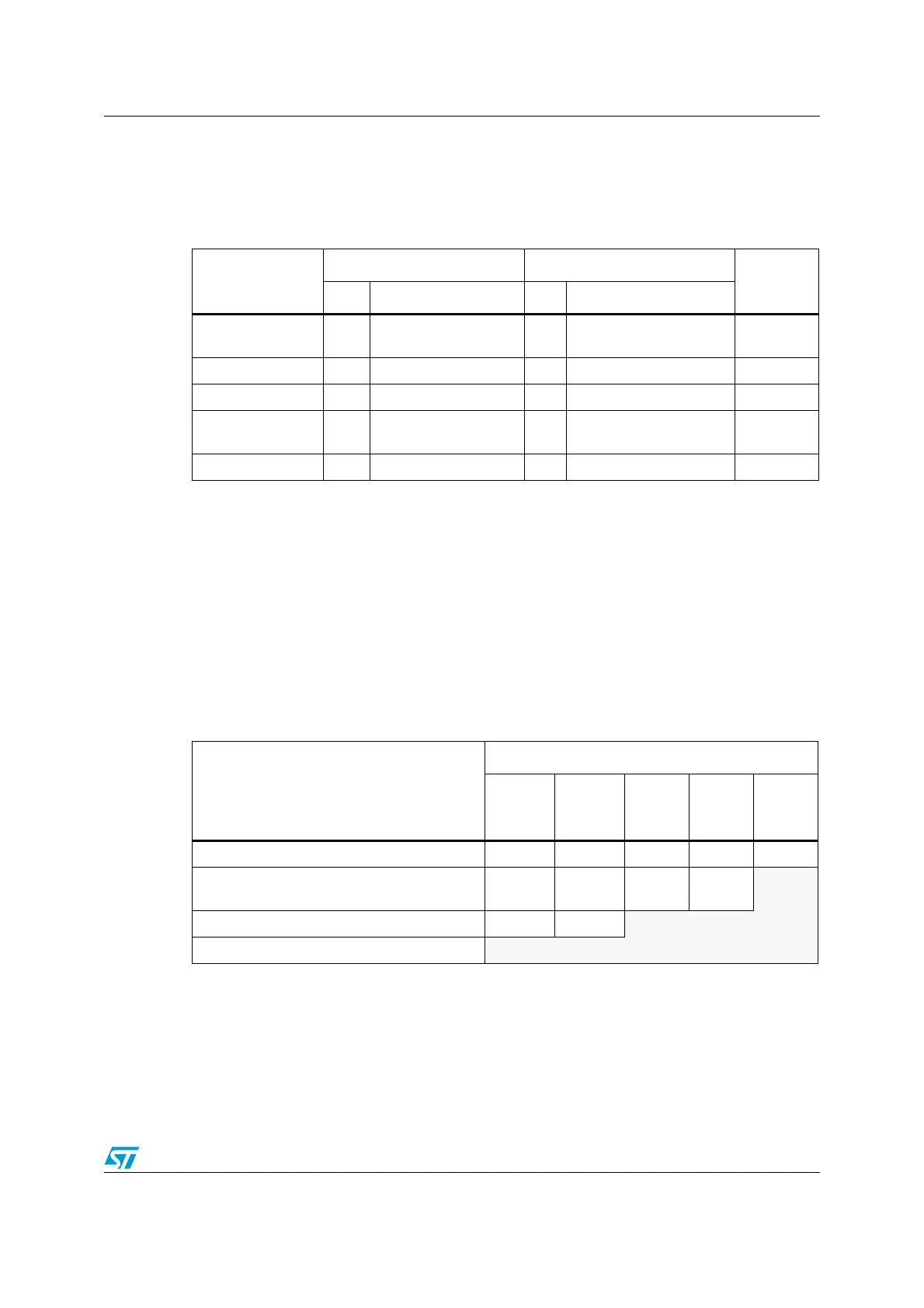
Table 2. Debug port pin assignment
SWJ-DP pin name
JTAG debug port SW debug port
Pin
assignment
Type Description Type Debug assignment
JTMS/SWDIO I
JTAG test mode
selection
I/O
Serial wire data
input/output
PA 1 3
JTCK/SWCLK I JTAG test clock I Serial wire clock PA14
JTDI I JTAG test data input - - PA15
JTDO/TRACESWO O JTAG test data output -
TRACESWO if async trace
is enabled
PB3
JNTRST I JTAG test nReset - - PB4
Table 3. SWJ I/O pin availability
Available debug ports
SWJ I/O pin assigned
PA13 /
JTMS/
SWDIO
PA1 4 /
JTCK/
SWCLK
PA15 /
JTDI
PB3 /
JTDO
PB4/
JNTRST
Full SWJ (JTAG-DP + SW-DP) - reset state X X X X X
Full SWJ (JTAG-DP + SW-DP) but without
JNTRST
XXXX
JTAG-DP disabled and SW-DP enabled X X
JTAG-DP disabled and SW-DP disabled Released