AN3216 Reference design
Doc ID 17496 Rev 5 25/30
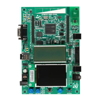
7 Reference design
7.1 Description
The reference design shown in Figure 15, is based on the STM32L152VB(T6).
This reference design can be tailored to any STM32L1xxx device with a different package,
using the pin correspondence given in Table 6: Reference connection for all packages.
7.1.1 Clock
Two clock sources are used for the microcontroller:
● LSE: X1– 32.768 kHz crystal for the embedded RTC
● HSE: X2– 8 MHz crystal for the STM32L1xxx microcontroller
Refer to Section 3: Clocks on page 14.
7.1.2 Reset
The reset signal in Figure 15 is active low. The reset sources include:
● Reset button (B1)
● Debugging tools via the connector CN1
Refer to Section 2.3: Reset and power supply supervisor on page 9.
7.1.3 Boot mode
The boot option is configured by setting switches SW2 (Boot 0) and SW1 (Boot 1). Refer to
Section 4: Boot configuration on page 18.
Note: In low-power mode (more specially in Standby mode) the boot mode is mandatory to be
able to connect to tools (the device should boot from the SRAM).
7.1.4 SWJ interface
The reference design shows the connection between the STM32L1xxx and a standard
JTAG connector. Refer to Section 5: Debug management on page 20.
Note: It is recommended to connect the reset pins so as to be able to reset the application from
the tools.
7.1.5 Power supply
Refer to Section 2: Power supplies on page 6.