Debug management AN3216
22/30 Doc ID 17496 Rev 5
5.3.3 Internal pull-up and pull-down resistors on JTAG pins
The JTAG input pins must not be floating since they are directly connected to flip-flops which
control the debug mode features. Special care must be taken with the SWCLK/TCK pin that
is directly connected to the clock of some of these flip-flops.
To avoid any uncontrolled I/O levels, the STM32L1xxx embeds internal pull-up and pull-
down resistors on the JTAG input pins:
● JNTRST: internal pull-up
● JTDI: internal pull-up
● JTMS/SWDIO: internal pull-up
● TCK/SWCLK: internal pull-down
Once a JTAG I/O is released by the user software, the GPIO controller takes control again.
The reset states of the GPIO control registers put the I/Os in the following equivalent states:
● JNTRST: input pull-up
● JTDI: input pull-up
● JTMS/SWDIO: input pull-up
● JTCK/SWCLK: input pull-down
● JTDO: input floating
The software can then use these I/Os as standard GPIOs.
Note: The JTAG IEEE standard recommends to add pull-up resistors on TDI, TMS and nTRST
but, there is no special recommendation for TCK. However, for the STM32L1xxx, an
integrated pull-down resistor is used for JTCK.
Having embedded pull-up and pull-down resistors removes the need to add external
resistors.
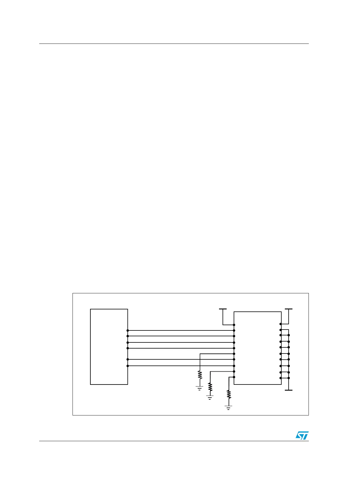
5.3.4 SWJ debug port connection with standard JTAG connector
Figure 13 shows the connection between the STM32L1xxx and a standard JTAG connector.
Figure 13. JTAG connector implementation
AIB
6
$$
6
$$
34-,XXX
N*4234
*4$)
*34-37$)/
*4#+37#,+
*4$/
N234).
642%&
N4234
4$)
4-3
4#+
24#+
4$/
N3234
$"'21
$"'!#+
K½
K½
K½
6
33
#ONNECTOR§
*4!'CONNECTOR#.