DocID027916 Rev 2 33/79
UM1902 Connector
78
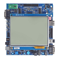
6.5 Daughterboard extension connector CN5 and CN6
Two 60-pin male headers CN5 and CN6 can be used to connect with daughterboard or
standard wrapping board to STM32746G-EVAL evaluation board. All GPIOs are dispatched
on memory connectors (CN10 and CN11), and on connectors CN5 and CN6.
The space between CN5 and CN6 connectors is defined as a standard, this allows
developing common daughterboards for several ST evaluation boards. The standard width
between CN5 pin1 and CN6 pin1 is 2700 mils (68.58 mm).
Each pin on CN5 and on CN6 can be used by a daughterboard, after disconnecting it from
the corresponding function block on STM32746G-EVAL evaluation board. Refer to Table 21
and Table 22 for details.
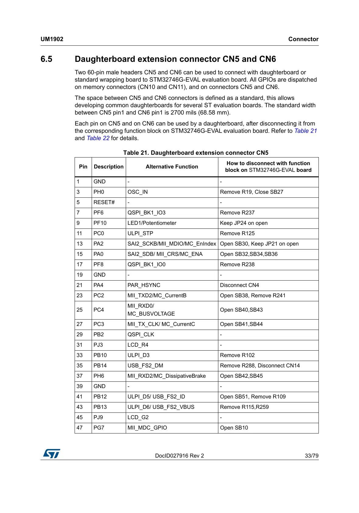
Table 21. Daughterboard extension connector CN5
Pin Description Alternative Function
How to disconnect with function
block on STM32746G-EVAL board
1GND - -
3 PH0 OSC_IN Remove R19, Close SB27
5 RESET# - -
7 PF6 QSPI_BK1_IO3 Remove R237
9 PF10 LED1/Potentiometer Keep JP24 on open
11 PC0 ULPI_STP Remove R125
13 PA2 SAI2_SCKB/MII_MDIO/MC_EnIndex Open SB30, Keep JP21 on open
15 PA0 SAI2_SDB/ MII_CRS/MC_ENA Open SB32,SB34,SB36
17 PF8 QSPI_BK1_IO0 Remove R238
19 GND - -
21 PA4 PAR_HSYNC Disconnect CN4
23 PC2 MII_TXD2/MC_CurrentB Open SB38, Remove R241
25 PC4
MII_RXD0/
MC_BUSVOLTAGE
Open SB40,SB43
27 PC3 MII_TX_CLK/ MC_CurrentC Open SB41,SB44
29 PB2 QSPI_CLK -
31 PJ3 LCD_R4 -
33 PB10 ULPI_D3 Remove R102
35 PB14 USB_FS2_DM Remove R288, Disconnect CN14
37 PH6 MII_RXD2/MC_DissipativeBrake Open SB42,SB45
39 GND - -
41 PB12 ULPI_D5/ USB_FS2_ID Open SB51, Remove R109
43 PB13 ULPI_D6/ USB_FS2_VBUS Remove R115,R259
45 PJ9 LCD_G2 -
47 PG7 MII_MDC_GPIO Open SB10