DocID030906 Rev 2 29/78
UM2271 Connectors
77
1. The 3V3 on ARD connector PIN4 is not a power input for 32L4R9IDISCOVERY board, to simplify power architecture.
2. The external voltage applied to pin VIN should be in the range 6 to 9V at 25°C ambient temperature. If a higher voltage is
applied on the regulator U15, it may overheat and could be damaged.
3. By default, pin 5 and pin 6 of CN17 connector are connected to ADC MCU input ports PA0 and PA5 respectively, thanks to
configuration of solder bridges: SB33 and SB35 closed, SB32 and SB34 opened. In case it is necessary to connect I2C
interface signals on pins 5 and 6 of CN17 instead of ADC inputs, open SB33 and SB35, and close SB32 and SB34.
VREF+, the voltage reference used by the internal DAC and ADC of STM32L4R9AI, has
three different power sourcing capabilities:
• from STM32L4R9AI MCU Internal buffer generation (Default). VREFBUF internal ADC
/ DAC voltage reference is set to 2.5V by default.
• from an external Arduino shield, connected to connector CN10. In that case, SB27
needs to be connected to bring AVDD on VREF+, a 100nF is necessary on C48 and
VREFBUF needs to be de-activated.
• from a VDDA power supply generated on 32L4R9IDISCOVERY board. VDDA is also
connected to VDDUSB of STM32L4R9AI. In that case, mounting a 0 ohm resistor on
R14 is necessary. VREFBUF needs to be de-activated. A jumper JP3 also needs to be
set as below description.
Warning: When VDDA=VDD_MCU and if VDD_MCU=1.8 V (check JP7
setting), there will be huge leakage current and a risk of
damaging MCU I/Os in case 3.3 V logic level is connected to
ADC input I/Os of STM32L4R9AI. Also, ADC measurements
will not be functional in default configuration
Caution: The I/Os of STM32 microcontroller are 3V3 compatible instead of 5 V for Arduino Uno.
Note: Limitation: the Arduino Uno Revision 3 is not compatible with JP7 setting at +1V8.
See Appendix B: Solder bridges for possible Arduino configuration change.
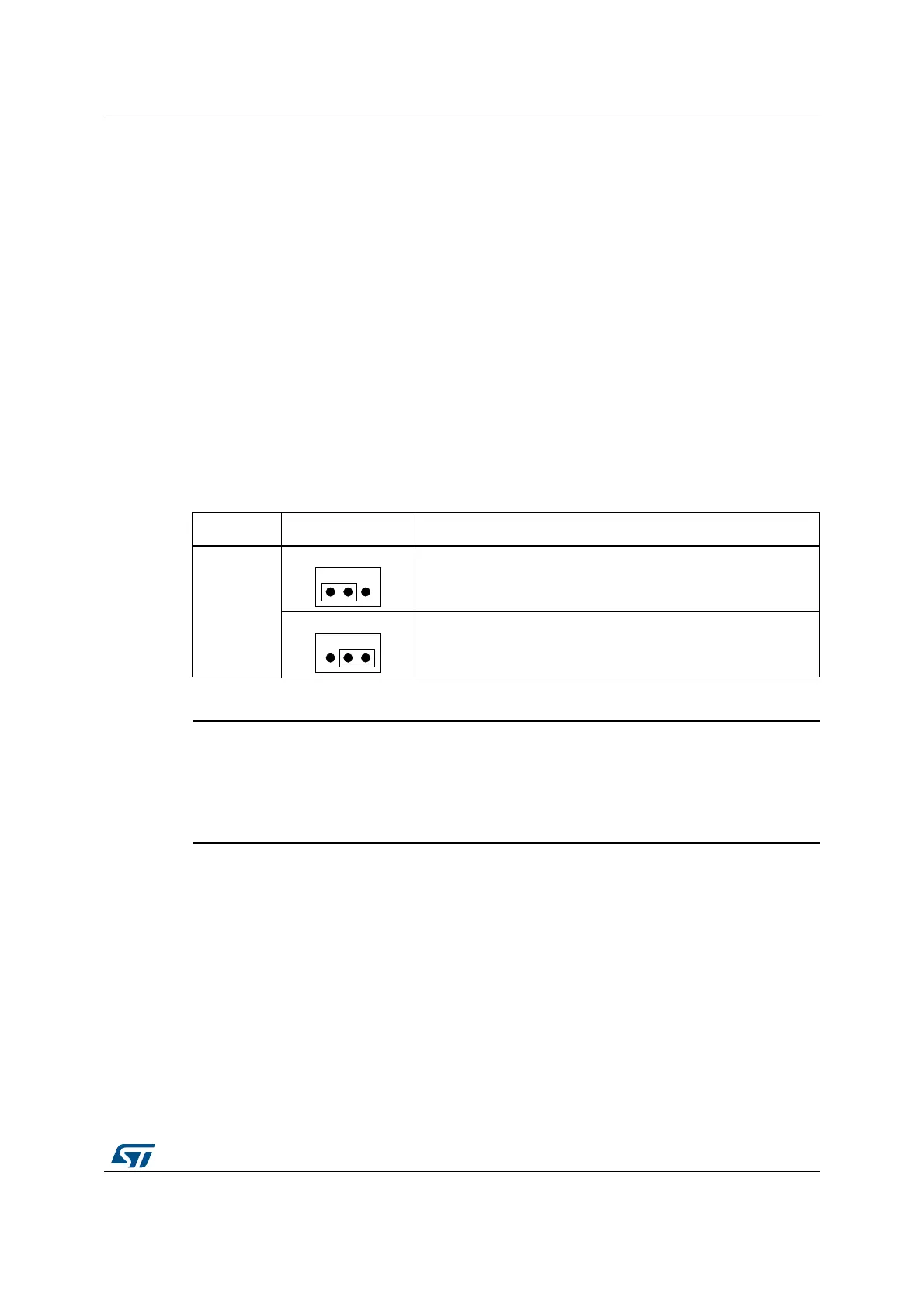
Table 14. JP3, VDDA and VDDUSB, settings
Jumper Setting Description
JP3
VDDA
Setting
Default setting.
Jumper on PIN1/2, VDDA get power from +3V3
Jumper on PIN2/3, VDDA get power form VDD_MCU
(See warning below)