DocID030906 Rev 2 31/78
UM2271 Connectors
77
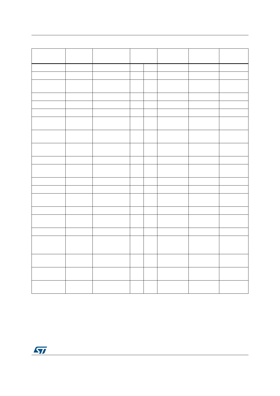
See Appendix B: Solder bridges for possible DSI display configuration change.
Power output - +5v 23 24 SPI2_SCK PB13 SPI clock
- - NC 25 26 SPI2_MOSIp PB15 SPI data
SM3321 ground - BLGND 27 28 SPI_DCX PB14
SPI
data/control
SM3321 ground - BLGND 29 30 NC - -
- - NC 31 32 RESERVED - -
- - NC 33 34 NC - -
- - NC 35 36 3V3 -
3V3 voltage
reference
- - NC 37 38 VDDIO -
IOVDD
reference
- - NC 39 40 I2C1_SDA PG13
Touch panel
I2C data
- - NC 41 42 NC - -
DSI_SWIRE
control output
PA8 DSI_SWIRE 43 44 I2C1_SCL PB6
Touch panel
I2C clock
- - NC 45 46 NC - -
- - NC 47 48 NC - -
DSI tearing
effect input
PF11 TE 49 50 NC - -
- - NC 51 52 NC - -
DSI Backlight
control output
PB1 DSI_BL_CTRL 53 54 NC - -
- - NC 55 56 NC - -
DSI and Touch
panel Reset
output
MFX_
GPIO10
DSI_RESET 57 58 NC - -
- - NC 59 60 1V8 -
1.8V voltage
reference
General ground - GND 61 62 GND -
General
ground
General ground - GND 63 64 GND -
General
ground
Table 15. DSI display connector CN4 (continued)
Function GPIO port Signal name
CN6 pin
number
Signal name GPIO port Function