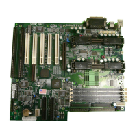
2-8
PDSBA-Q+/PDSBA+/PDSBA/PDSBE User's Manual
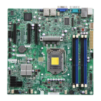
S
UPER PDSBA+
®
Processor
JPWAKE
4-PinPWR
KB/MS
USB3/4/5/6
USB1/2
LAN
Fan3
Clock
Intel
North Bridge
PCI-E x1
PCI-E x16
PCI-E x4
PCI-33MHz
LAN
CTRL
JPL1
COM2
FWH
JL1
JWOR
I-SATA0
I-SATA1
FP CT
RL
Fa
n
2
Buzzer
24-Pin A
T
X
P
W
R
Sup
er
IO
Fan1/CPU Fan
Intel
J44
DIMM#1A (Blue)
DIMM#2A (Black)
DIMM#1B (Blue)
DIMM#2B (Black)
Floppy
Audio
WOL
JBT1
South Bridge
J12
Battery
J
PUSB1
JPUSB
2
COM1
JF
SB1
JF
SB2
Slot7
Slot6
Slot5
Slot4
JI
2
C1
JI
2
C2
PCI-33MHz
Slot3
PCI-33MHz
Slot2
Slot1
PCI-33MHz
J
9
I-SATA4
I-SATA5
RAIDLED
USB7/8
J45
USB9/10
LE1
JLED
JWD
CD1
Parallel Port
VGA
HDA
IDE#2
IDE#1
ITE
J
P
2
JP3
Power Button
OH/Fan Fail LED
1
NIC1 LED
Reset Button
2
HDD LED
Power LED
Reset
PWR
LED_Anode
LED_Anode
LED_Anode
LED_Anode
Ground
Ground
X
X
X
X
Power LED
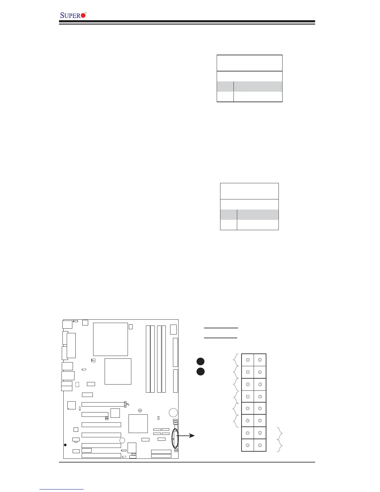
The Power LED connection is located
on pins 15 and 16 of JF1. Refer to the
table on the right for pin defi nitions.
Power LED
Pin Defi nitions (JF1)
Pin# Defi nition
15 LED_Anode
16 PWR LED Signal
Front Control Panel Pin Defi nitions
A. PWR LED
B. HDD LED
HDD LED
The HDD LED connection is located
on pins 13 and 14 of JF1. Attach a
hard drive LED cable here to display
disk activity (for any hard drives on
the system, including SAS and Serial
ATA). See the table on the right for
pin defi nitions.
HDD LED
Pin Defi nitions (JF1)
Pin# Defi nition
13 LED_Anode
14 HD Active
A
B