2-26
PDSBA-Q+/PDSBA+/PDSBA/PDSBE User's Manual
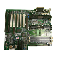
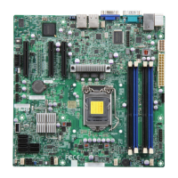
S
UPER PDSBA+
®
Processor
JPWAKE
4-PinPWR
KB/MS
USB3/4/5/6
USB1/2
LAN
Fan3
Clock
Intel
North Bridge
PCI-E x1
PCI-E x16
PCI-E x4
PCI-33MHz
LAN
CTRL
JPL1
COM2
FWH
JL1
JWOR
I-SATA0
I-SATA1
F
P CTRL
Fa
n
2
Buzzer
24-Pin ATX PW
R
S
up
er IO
Fan1/CPU Fan
Intel
J44
DIMM#1A (Blue)
DIMM#2A (Black)
DIMM#1B (Blue)
DIMM#2B (Black)
Floppy
Audio
WOL
JBT1
South Bridge
J12
Battery
J
PUSB1
J
PUSB2
COM1
JF
SB1
J
FSB2
Slot7
Slot6
Slot5
Slot4
JI
2
C1
JI
2
C2
PCI-33MHz
Slot3
PCI-33MHz
Slot2
Slot1
PCI-33MHz
J9
I-SATA4
I-SATA5
RAIDLED
USB7/8
J45
USB9/10
LE1
JLED
JWD
CD1
Parallel Port
VGA
HDA
IDE#2
IDE#1
ITE
J
P2
JP3
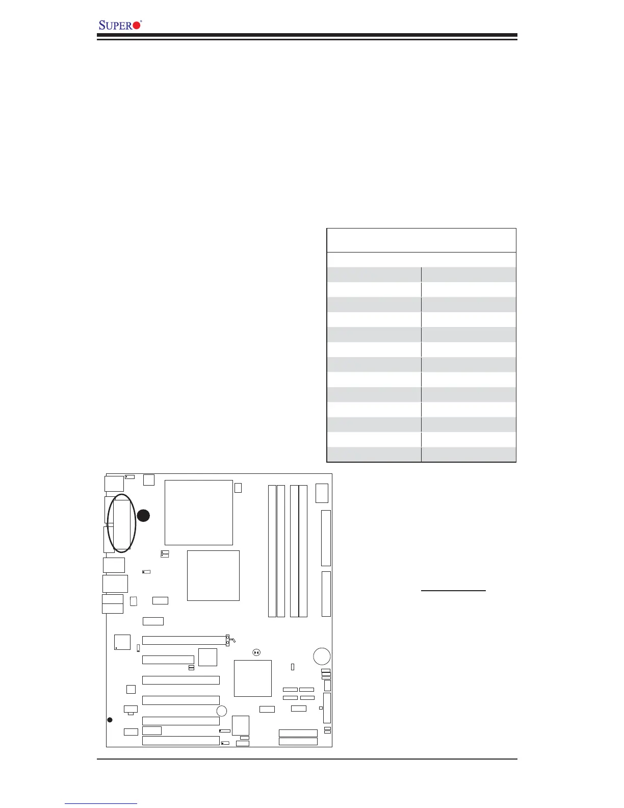
Parallel (Printer) Port Connector
The parallel (printer) port is located
at J30. See the table on the right for
pin defi nitions.
2-9 Parallel Port, Floppy Drive and IDE Hard Drive
Connections
Note the following when connecting the fl oppy and hard disk drive cables:
• The fl oppy disk drive cable has seven twisted wires.
• A red mark on a wire typically designates the location of pin 1.
• A single fl oppy disk drive ribbon cable has two connectors to provide for two
fl oppy disk drives. The connector with twisted wires always connects to drive
A, and the connector that does not have twisted wires always connects to drive
B.
Parallel (Printer) Port Connector
Pin Defi nitions
Pin# Defi nition Pin # Defi nition
1 Strobe- 2 Auto Feed-
3 Data Bit 0 4 Error-
5 Data Bit 1 6 Init-
7 Data Bit 2 8 SLCT IN-
9 Data Bit 3 10 GND
11 Data Bit 4 12 GND
13 Data Bit 5 14 GND
15 Data Bit 6 16 GND
17 Data Bit 7 18 GND
19 ACK 20 GND
21 BUSY 22 Write Data
23 PE 24 Write Gate
25 SLCT 26 NC
A
A. Parallel Port