Chapter 2: Installation
2-15
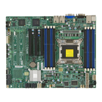
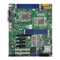
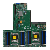
JTPM1
JIPMB1
S4
I-SATA3
I-SATA0
I-SATA1
JPL1
JPUSB1
JLED1
JVR2
JVR1
JPG1
JPAC1
JBT1
JSTBY1
JSD1
JF1
Rev. 1.00
BIOS
LICENSE
FOR HOME OR OFFICE USE
With FCC Standards
Tested to Comply
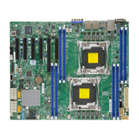
JPW2
JL1
JL2
JI2C1
JSPDIF_OUT
JPW1
MAC CODE
BAR CODE
JITP1
LEDM1
SP1
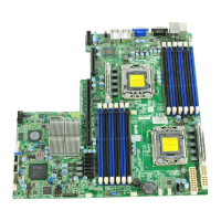
FAN3
FAN2
FAN4
FAN1
FAN5
JD1
JAUDIO1
JBR1
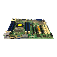
USB8/9(3.0)
OC_FRONT_PANEL
(3.0)
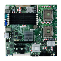
I-SATA0
I-SATA1
I-SATA2
I-SATA3
I-SATA4
I-SATA5
(3.0)
USB 2/3
USB 12/13
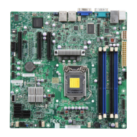
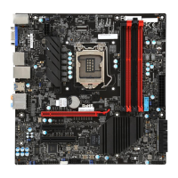
FAN1/CPU
PCH_SLOT2 PCI-E 2.0 X4
LAN
HDMI/DP
KB/MOUSE
AUDIO FP
DIMMB1
DIMMB2
HD AUDIO
USB4/5
USB6/7
DIMMA1
DIMMA2
CPU_SLOT1 PCI-E 3.0 X8
CPU_SLOT3 PCI-E 3.0 X16
COM1
VGA(IPMI)
USB 0/1
JI2C2
C7Z97-M
JPME2
JWD1
S8
S11
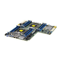
A. Backpanel USB 2.0 #0
B. Backpanel USB 2.0 #1
C. Backpanel USB 3.0 #2
D. Backpanel USB 3.0 #3
E. Backpanel USB 3.0 #12
F. Backpanel USB 3.0 #13
G. USB 2.0 Header #4/5
H. USB 2.0 Header #6/7
I. USB 3.0 Header #14/15
Universal Serial Bus (USB)
Two Universal Serial Bus 2.0 ports (0/1) and four USB 3.0 ports
(2/3,12/13) are located on the I/O back panel. In addition, two USB
2.0 headers (four ports: 4/5, 6/7), and one USB 3.0 header (two ports:
14/15) are also located on the motherboard to provide front chassis
access using USB cables (not included). See the tables below for pin
denitions.
Back Panel USB (2.0) #0/1, USB (3.0) #2/3,
12/13 Pin Denitions
Pin# Denition Pin# Denition
1 +5V 5 +5V
2 USB_PN1 6 USB_PN0
3 USB_PP1 7 USB_PP0
4 Ground 8 Ground
Front Panel USB (2.0) Header #4/5, 6/7
Pin Denitions
Pin # Denition Pin # Denition
1 +5V 2 +5V
3 USB_PN2 4 USB_PN3
5 USB_PP2 6 USB_PP3
7 Ground 8 Ground
9 Key 10 Ground
A
Front Panel USB (3.0) Header #14/15
Pin Denitions
Pin# Pin# Signal Name Description
1 10 VBUS Power
2 11 D- USB 2.0 Differential Pair
3 12 D+
4 13 Ground Ground of PWR Return
5 14 StdA_SSRX- SuperSpeed Receiver
6 15 StdA_SSRX+ Differential Pair
7 16 GND_DRAIN Ground for Signal Return
8 17 StdA_SSTX- SuperSpeed Transmitter
9 18 StdA_SSTX+ Differential Pair
C
E
B
 Loading...