51
Chapter 2: Installation
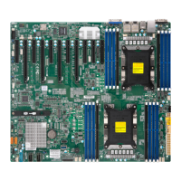
S-SGPIO Header
A Serial General Purpose Input/Output header (S-SGPIO) is located on the motherboard.
This header is used to communicate with the enclosure management chip on the backplane.
Refer to the table below for pin denitions.
SGPIO Header
Pin Denitions
Pin# Denition Pin# Denition
1 NC 2 NC
3 Ground 4 DATA Out
5 Load 6 Ground
7 Clock 8 NC
NC = No Connection
Disk-On-Module Power Connector
The Disk-On-Module (DOM) power connectors at JSD1 and JSD2 provide 5V power to a
solid-state DOM storage devices connected to one of the SATA ports. Refer to the table
below for pin denitions.
DOM Power
Pin Denitions
Pin# Denition
1 5V
2 Ground
3 Ground
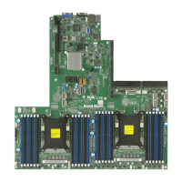
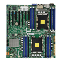
1. S-SGPIO
2. JSD1
3. JSD2
X11DPG-QT
DESIGNED IN USA
REV:1.10A
IPMI CODE
MAC CODE
SAN MAC
BAR CODE
BIOS
LICENSE
CPU1
CPU2
JBT1
PCH
BT1
BMC
VGA
COM1
USB 0/1
IPMI_LAN
USB 4/5 (3.0)
LAN 1
LAN 2
FAN 3
FAN 4
FAN 6
FAN 1
FAN 5
FAN 2
FAN A
FAN B
P2-DIMMD2
P2-DIMMD1
P2-DIMME1
P2-DIMMF1
P1-DIMMA2
P1-DIMMA1
P1-DIMMB1
P1-DIMMC1
JUIDB1
(UID)
LED2
(UID-LED)
LEDM1
JPWR1
JPWR2
JPWR3
LAN
CTRL
P1-DIMMF1
P1-DIMME1
P1-DIMMD1
P1-DIMMD2
P2-DIMMC1
P2-DIMMB1
P2-DIMMA1
P2-DIMMA2
JNCSI1
JTBT1
JPCIE11
JPCIE10
(CPU2 SLOT11 PCI-E 3.0 x4 (IN x8))
(CPU2 SLOT10 PCI-E 3.0 x16)
JPCIE8
JPCIE9
(CPU2 SLOT8 PCI-E 3.0 x16)
JNVI2C2
JNVI2C1
(CPU1 SLOT9 PCI-E 3.0 x16)
JPCIE6
JPCIE4
(CPU2 SLOT6 PCI-E 3.0 x16)
(CPU1 SLOT4 PCI-E 3.0 x16)
JPCIE2
(CPU1 SLOT2 PCI-E 3.0 x16)
JGPIO_P2: CPU2-HSSI GPIO
JGPIO_P1: CPU1-HSSI GPIO
S-UM12
JPI2C1
JPWR4
LEDPWR
JF1
JHD_AC1
AUDIO_FP
JSPDIF_IN1
JPAC1
JPME2
JTPM1
COM2
JPTG1
JRK1
JIPMB1
JVRM_SEL1
JWD1
JSEN1
JSTBY1
I-SATA0~3I-SATA4~7
USB 6/7 (3.0)
USB 2/3
S-SATA4
S-SATA5
USB8 (3.0)
SP1
M.2 CONNECTOR
JSD1
JSD2
S-SGPIO
JL1
FAN C FAN D
1
2
3
 Loading...