2-22
X9SRL Motherboard Series User’s Manual
1
JD1
7
JIPMB1
C
A
4
5
8
1
JPW2
I-SATA5
I-SATA4
I-SATA3
I-SATA2
2
UID_SW
1
DIMM_C1DIMM_C2DIMM_D1
DIMM_A1
DIMM_B1
DIMM_A2
DIMM_B2
DIMM_D2
I-SATA1
I-SATA0
I-SAS3
I-SAS2
I-SAS1
I-SAS0
7
JVGA
2
1
JF1
19
20
JKBMS1
C
A
UID_LED
JLAN_USB12
X_BT1
+
5
JPI2C1
1
JBT1
1
JPW1
13
JUSB2
3-SGPIO1
2
8
T-SGPIO2 T-SGPIO1
JOH1
1
JL1
1
JI2C2
1
JI2C1
A
DP3
CA
JPBIOS1
JPME1
1
JIBTN1
3
1
3
JWD1
JVR2
3
1
JPL2
1
JPL1
1
3
JVR1
1
3
1
JPUSB1
3
3
JPG1
1
JPB1
1
FANA
FAN5
1
4
FAN3
FAN4
1
FAN2
4
1
FAN1
4
MH11
MH1
MH5
MH9
MH8
MH2
MH10
JCOM1
PCIE6
PCIE5
PCIE4
PCIE3
PCIE7
2
JTPM1
PCIE1
PCIE2
JPK1
1
3
JSD1
JSTBY1
1
3
JLAN1
JLAN2
REV:1.00
Tested to Comply
With FCC Standards
FOR HOME OR OFFICE USE
DESIGNED IN USA
BAR CODE
JCOM2
1
5
6
9
1
7
2
JUSB45
1
7
2
JUSB67
1
7
JUSB89
P1-DIMM2D
P1-DIMM2C
P1-DIMM1C
P1-DIMM1D
P1-DIMM2B
P1-DIMM2A
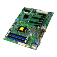
CPU1
SLOT7 PCI-E 3.0X8 (INX8)
SLOT6 PCI-E 3.0X8 (INX16)
SLOT5 PCI-E 3.0X8 (INX8)
SLOT4 PCI-E 3.0X8 (INX16)
SLOT3 PCI-E 3.0X4 (INX8)
SLOT2 PCI-E 3.0X4 (INX8)
SLOT1 PCI-E 2.0X4 (INX8)
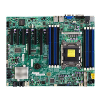
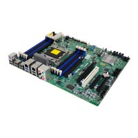
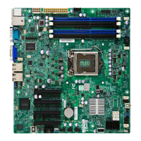
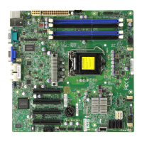
X9SRL
JPK1
JPME1
JBT1 COMS CLEAR
JPBIOS1
JL1 CHASSIS INTRUSION
JSD1:SATA DOM POWER
JPI2C1:PWRI2C
JTPM1:TPM/PORT80
ON:ME RECOVEROS
OFF:NORMAL
COM2
Pin1:RAID_KEY_PCH
Pin3:PCH_DYN_SKU
Pin2:Ground
JPB1
1-2 Enable
2-3 Disable
1-2:NORMAL
2-3:RECOVER BIOS
1-2 Enable
2-3 Disable
JPG1: VGA
OFF:DISABLE
JI2C1/JI2C2
ON: ENABLE
UID
RST
ON
PWR
LAN2
PWR
FF
OH
FAIL
HDD
LED
PWR
X
NIC
1
2
NIC
NMI
LAN1
2-3:NMI
1-2:RST
2-3 Disable
1-2 Enable
JWD1:Watch Dog
JPL1/2: LAN
PWR LED
SPEAKER
1-3:
4-7:
JD1:
VGA
COM1
IPMI_LAN
USB0/1
2-3 ENable
P1-DIMM1B
KB/MOUSE
1-2 Disable
JPUSB1:USB Wake Up
P1-DIMM1A
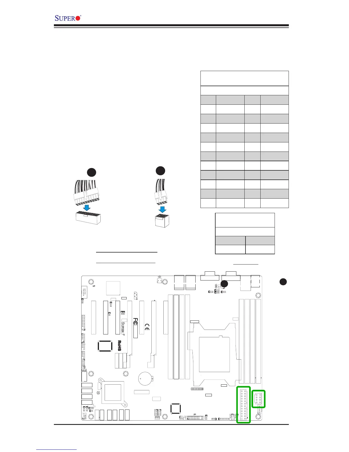
2-6 Connecting Cables & Optional Devices
This section provides brief descriptions and pin-out denitions for onboard headers
and connectors. Be sure to use the correct cable for each header or connector.
A. 24-Pin ATX Main PWR
B. 8-Pin Processor PWR
A
B
ATX Power 24-pin Connector
Pin Denitions (JPW1)
Pin# Denition Pin # Denition
13 +3.3V 1 +3.3V
14 -12V 2 +3.3V
15 COM 3 COM
16 PS_ON 4 +5V
17 COM 5 COM
18 COM 6 +5V
19 COM 7 COM
20 Res (NC) 8 PWR_OK
21 +5V 9 5VSB
22 +5V 10 +12V
23 +5V 11 +12V
24 COM 12 +3.3V
(Required)
12V 8-pin Power Connec-
tor Pin Denitions
Pins Denition
1 through 4 Ground
5 through 8 +12V
ATX Main PWR (JPW1) & CPU PWR
Connectors (JPW2)
The 24-pin main power connector (JPW1) is
used to provide power to the motherboard.
The 8 -pin CPU PWR connector (JPW2) is also
required for the processor. These power con-
nectors meet the SSI EPS 12V specication.
See the table on the right for pin denitions.
8-Pin Processor PWR
A
B
24-Pin Main PWR