1-8
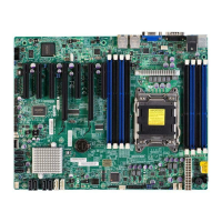
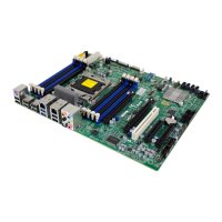
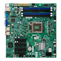
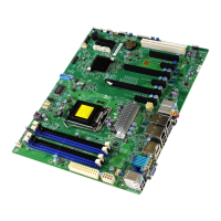
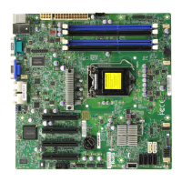
X9SRL Motherboard Series User’s Manual
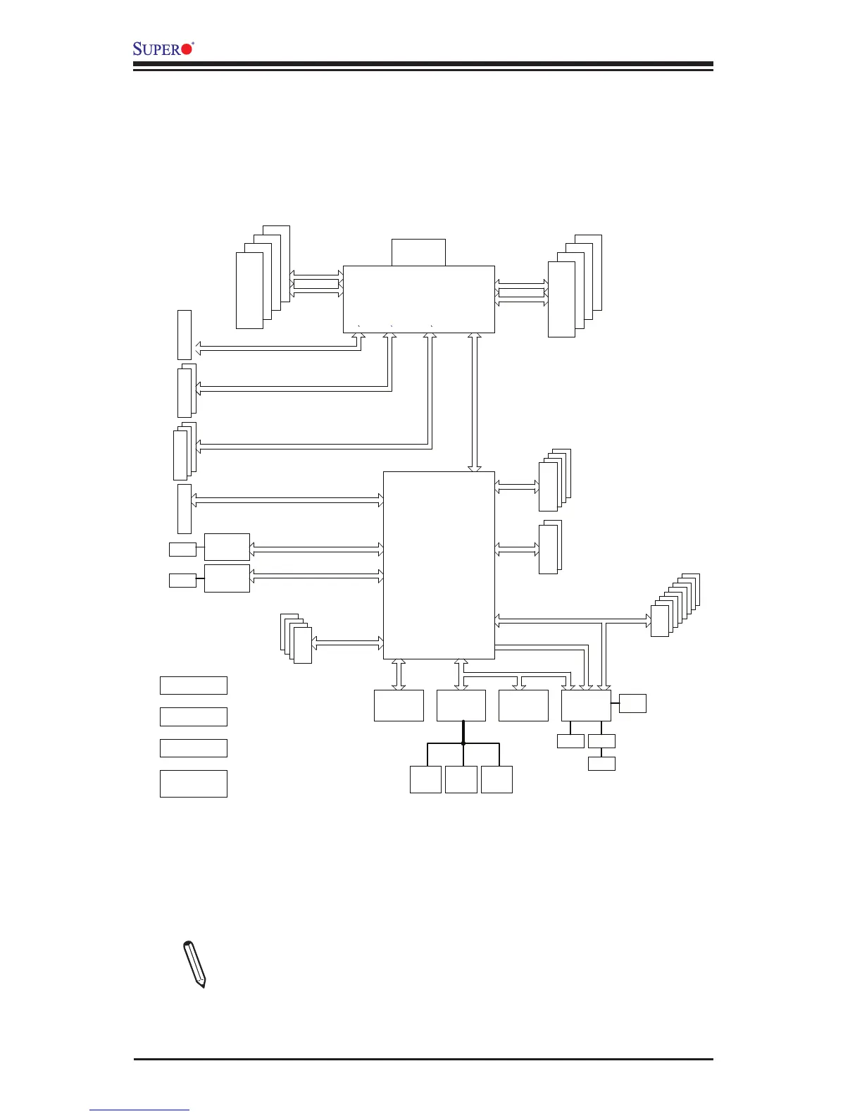
System Block Diagram
Note: This is a general block diagram and may not exactly represent the
features on your motherboard. See the Motherboard Features pages for
theactualspecicationsofeachmotherboard.
Motherboard Block Diagram
SLOT 7
82574L
SLOT 3
#8
COM1
Rear
6 PHASE
X9SRL
800/1066/1333
800/1066/1333
DDRIII
VR12
#0-4
#0-3
#0-2
#0-1
DDRIII
#0-8
#0-7
#0-6
#0-5
#6
#7
COM2
Header
SLOT 1/5
USB 2.0
6.0 Gb/S
Intel E5-1600/2600
PCH
Intel C602
SSB-A
1X "PCI-E X8 G3"
BIOS
SIO
NCT6776F
LPC
USB
#0
#1
#2
#4
#5
SATA
#0
#1
FRONT PANEL
SYSTEM POWER
DEBUG
PORT
FAN SPEED
CTRL
PCI-E X4 G2
PCI-E X8
LAN#1
PCI-E X8
8 SNB CORE
DDR-III
MAX 130W
#1A
B #2A/B C/D
#1B
DMI2
#3A/B
C/D
1X "PCI-E X8 G3" 2X "PCI-E X4 G3"
PCI-E X1
#4
#5
3.0 Gb/S
SATA
#2
#3
3.0 Gb/S
SATA
#0
#1
#2
#3
DMI2 4GB/s
BMC
WPCM450
SPI
TPM
HEADER
PCI
DDR2
VGA PHY
RJ45
RMII
RJ45
PCI-E X16
2X "PCI-E X8 G3"
#1/2/3/4
#7
#12
#13
PS/2
KB/MS
PCI-E X8
SLOT 2/5/6
82574LRJ45
LAN#2
PCI-E X1
#8
SCU