INSTALLATION
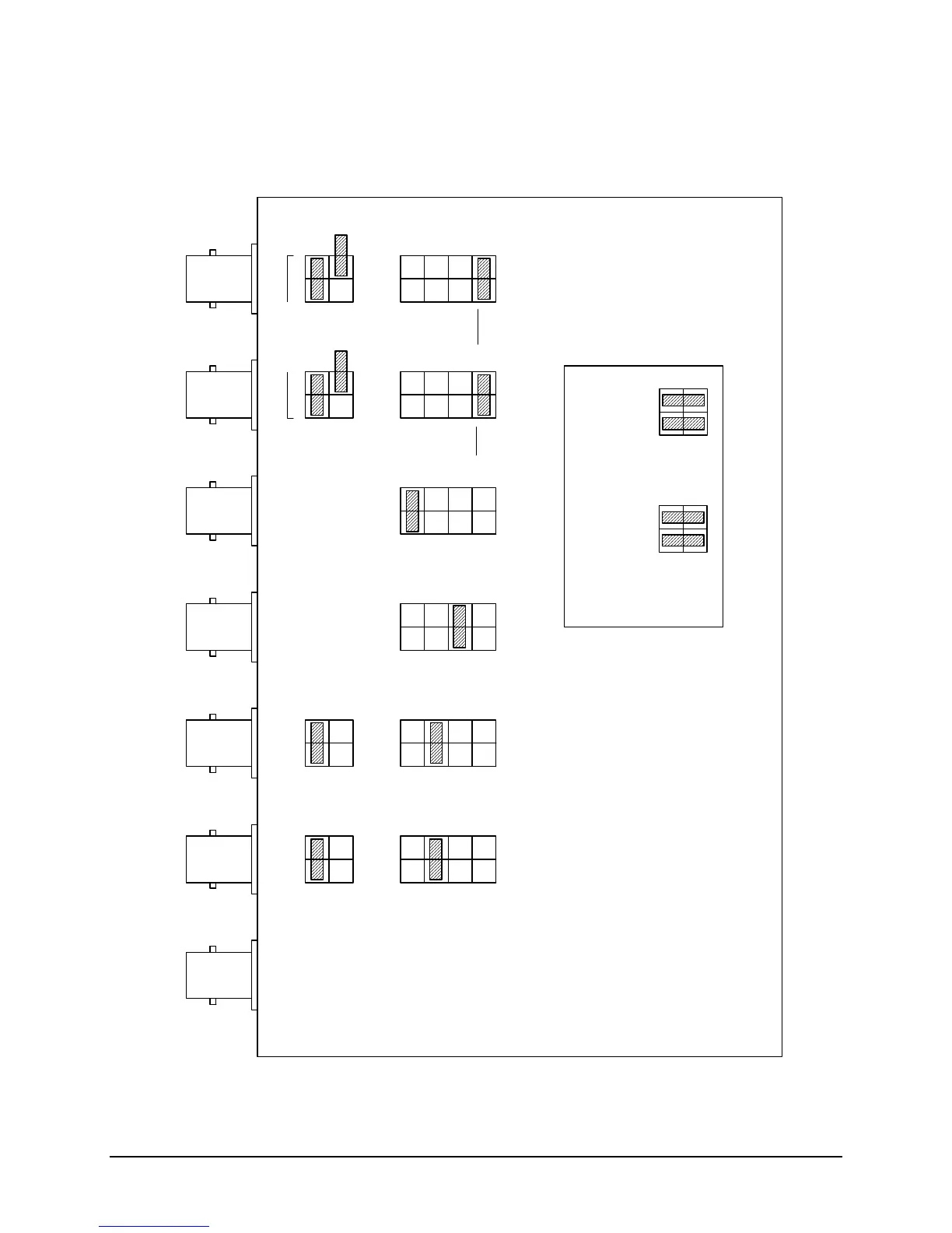
Figure 2-3
GPS Main Assembly 100015
6
J10
1
3 4
J29
1
3
2
4
Buffered Out -
Event 3 In -
Buffered Out -
Event 2 In
-
1
3
5
7 8
6
4
2
MUX Ch: 1 -
AC Code Out -
10 MHz Sine -
Unused -
1
3
5
7 8
6
4
2
MUX Ch: 2 -
AC Code Out -
10 MHz Sine -
Unused -
1
3
5
7 8
4
2
MUX Ch: 4 -
AC Code Out -
10 MHz Sine -
Unused -
1
3
5
7 8
6
4
2
MUX Ch: 3 -
AC Code Out -
10 MHz Sine -
Unused -
1
3
5
7 8
6
4
2
MUX Ch: 2 -
AC Code Out -
10 MHz Sine -
Locked-
1
3
5
7 8
6
4
2
MUX Ch: 1 -
AC Code Out -
10 MHz Sine -
Tracking -
Main GPS Board
Assembly 100015
Rear
2 1
3
2
4
Buffered Out -
1
3
2
4
Buffered Out -
Relay-
See Inset
Below
J24 & J25 above are jumpered for "Buffered
Outputs."
The diagram below illustrates the jumper positions
for "Relay Outputs."
Inset
Example: Inserting jumper blocks into J14-5&6, and J24-1&2 will output a 10 MHz sine wave on rear panel BNC connector J4.
Notes:
1. Mux Channel 1 can be output on both J4 and J9.
2. Mux Channel 2 can be output on both J5 and J8.
3. Shaded areas are the standard (default) configuration.
J9 J8
J7
J6 J5
J4
J28 J25
J24
Relay-
J14
J15
J16J17
J18J19
J25
1
3
2
4
Buffered Out -
Relay-
1
3
Buffered Out -
2
4
J24
Relay-
Time Interval Input
Ext. Freq. Measurement Input
Event 1 Input
Symmetricom Inc ET6xxx ExacTime GPS TC & FG (Rev C) 2-9
 Loading...