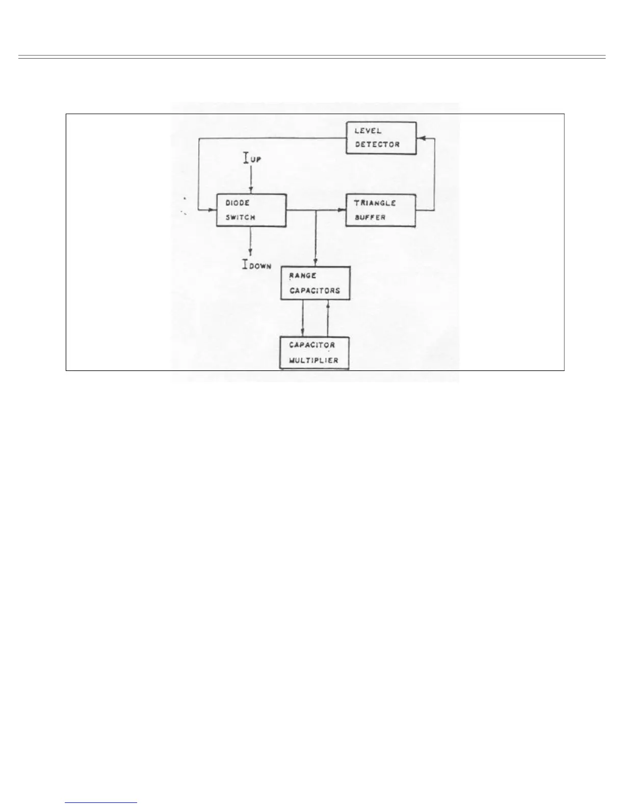
CAPACITOR MULTIPLIER
- The capacitor multi-
plier is used for the 2mHz to 19.9Hz ranges. The function
of this circuit is to generate an equivalent large capaci-
tance. The larger values of capacitors are required to gen-
erate lower frequencies. The capacitor multiplier is
formed by U40 ,U41 and their associated components.
The multiplier ratio is selected by changing the ranging
resistors in the negative feedback path of U40. The rang-
ing resistors are selected by Q43 and analog switch U42.
The switching control is provided by the serial to parallel
converter U38.
6-3-3. Sine Shaper
The sine shaper consists of a series of differential stages
which are formed by the transistor arrays U45, U46 and
U47. The differential stages are connected in parallel and
receive the drive signal from the triangle buffer output.
This circuit takes advantage of the non- linear charac-
teristics of the transistors and by biasing them to different
dc levels, the output of the common collector is shaped to
a sinewave. The sinewave is then amplified and re-biased
to oscillate around 0V with a differential amplifier which
is formed by Q34, Q35, Q36 and Q37, U45b, U45c and
their associated components.
6-3-4. Trigger Circuit
The trigger circuit is active when one of the trigger modes
is selected. The trigger circuit is composed of two main
sections: the clamp circuit and the trigger logic circuit.
Figure 6-4 is a simplified block diagram of the clamp cir-
cuit. Refer to this Figure and to the schematic diagrams at
the end of this manual throughout the following descrip-
tion. Detailed description of the clamp and the trigger
logic circuits is provided in the following. Description is
given for both trigger and gated modes.
CLAMP CIRCUIT
- The clamp circuit is composed of
U24, Q20, Q21 and their associated components. When
no trigger mode is selected, U24 is cleared with its inverted
Q output set to “1". At this time, the trigger current flows
through Q20. Q21, which is connected as a diode, is re-
versed biased and do not interfere with normal VCO op-
eration.
Selecting one of trigger or gated modes its inverted Q
output is modified to “0". The up current from the VCO
circuit is diverted through Q21 to the junction of Q20 and
Q21. Due to the fact that the Current from the trigger cur-
rent is double that of the up or down currents, the current
flow through Q20 will equal to that flowing through Q21.
Under these conditions, the clamp level, at the triangle
buffer input will be set to logical ”0" level. This sequence
Figure 6-3. VCO Simplified Block Diagram.
Theory Of Operation Model 8020
Page 6-4