Theory of Operation-314 Service
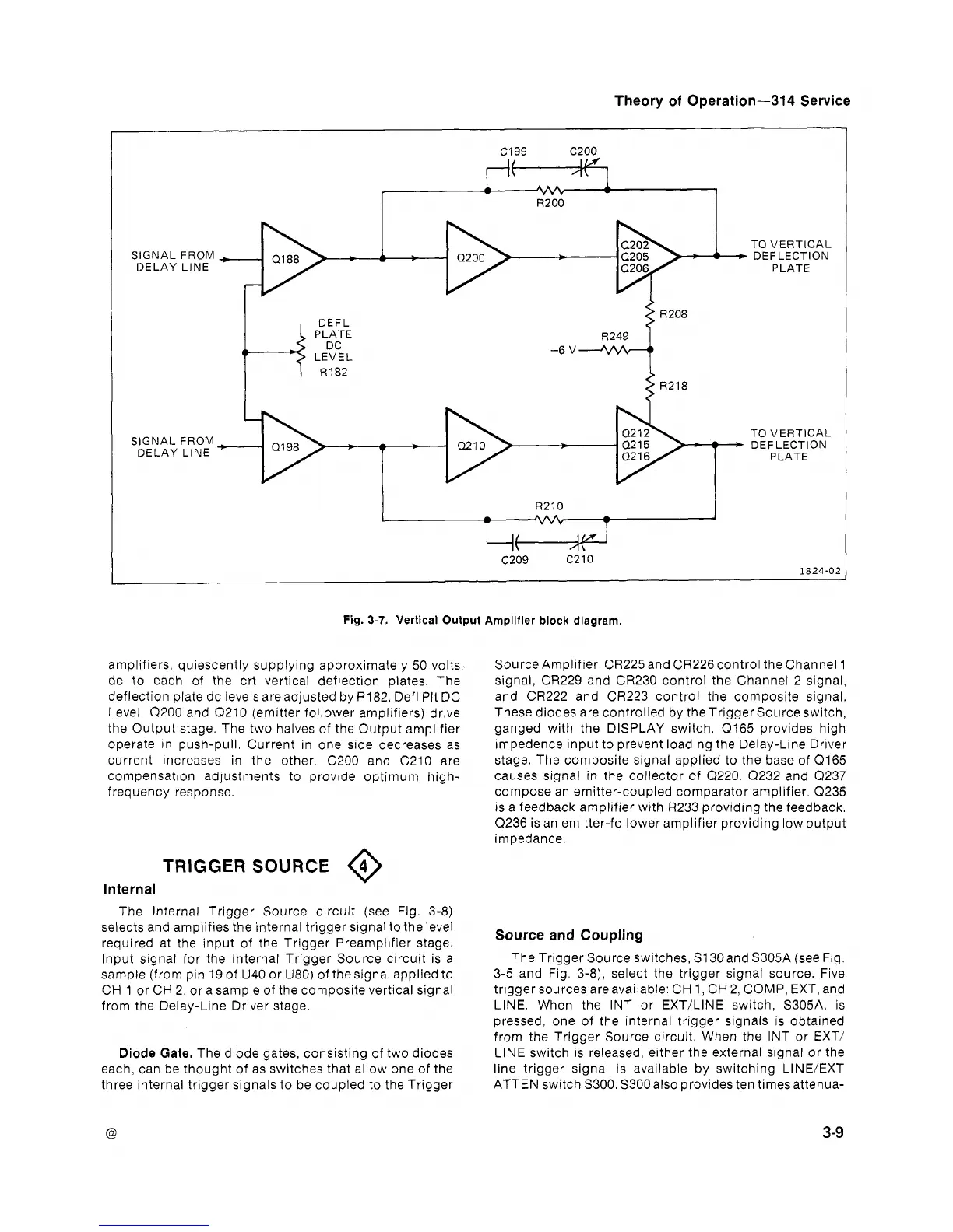
TO VERTICAL
SIGNAL FROM
-
-
-
-
-
-
A
-
+
DEFLECTION
DELAY LlNE
-
PLATE
r
LEVEL
SIGNAL FROM
-
-
-
-
TO
VERTICAL
DELAY LlNE
-
-
7
-
r
*
DEFLECTION
PLATE
Fig.
3-7.
Vertical Output Amplifier
block
diagram.
amplifiers, quiescently supplying approximately 50 volts
dc to each of the crt vertical deflection plates. The
deflection plate dc levels areadjusted by R182, Defl Plt DC
Level. Q200 and Q210 (emitter follower amplifiers) drive
the Output stage. The two halves of the Output amplifier
operate in push-pull. Current in one side decreases as
current increases in the other. C200 and C210 are
compensation adjustments to provide optimum
high-
frequency response.
TRIGGER SOURCE
@
Internal
The lnternal Trigger Source circuit (see Fig. 3-8)
selects and amplifies the internal trigger signal to the level
required at the input of the Trigger Preamplifier stage.
Input signal for the Internal Trigger Source circuit is a
sample (from pin 19 of U40 or U80) of thesignal applied to
CH
1
or CH 2, or a sample of the composite vertical signal
from the Delay-Line Driver stage.
Diode
Gate.
The diode gates, consisting of two diodes
each, can be thought of as switches that allow one of the
three internal trigger signals to be coupled to the Trigger
Source Amplifier. CR225 and CR226 control the Channel 1
signal, CR229 and CR230 control the Channel 2 signal,
and CR222 and CR223 control the composite signal.
These diodes are controlled by the Trigger Source switch,
ganged with the DISPLAY switch. Q165 provides high
impedence input to prevent loading the Delay-Line Driver
stage. The composite signal applied to the base of Q165
causes signal in the collector of (2220. Q232 and Q237
compose an emitter-coupled comparator amplifier. (223.5
is a feedback amplifier with R233 providing the feedback.
Q236 is an emitter-follower amplifier providing low output
impedance.
Source and Coupling
The Trigger Source switches, S130and S305A (see Fig.
3-5 and Fig. 3-8), select the trigger signal source. Five
trigger sources areavailable: CH 1, CH 2, COMP, EXT, and
LINE. When the INT or EXTILINE switch, S305A, is
pressed, one of the internal trigger signals is obtained
from the Trigger Source circuit. When the INT or EXT/
LlNE switch is released, either the external signal or the
line trigger signal is available by switching LINE/EXT
ATTEN switch S300. S300 also provides ten times attenua-