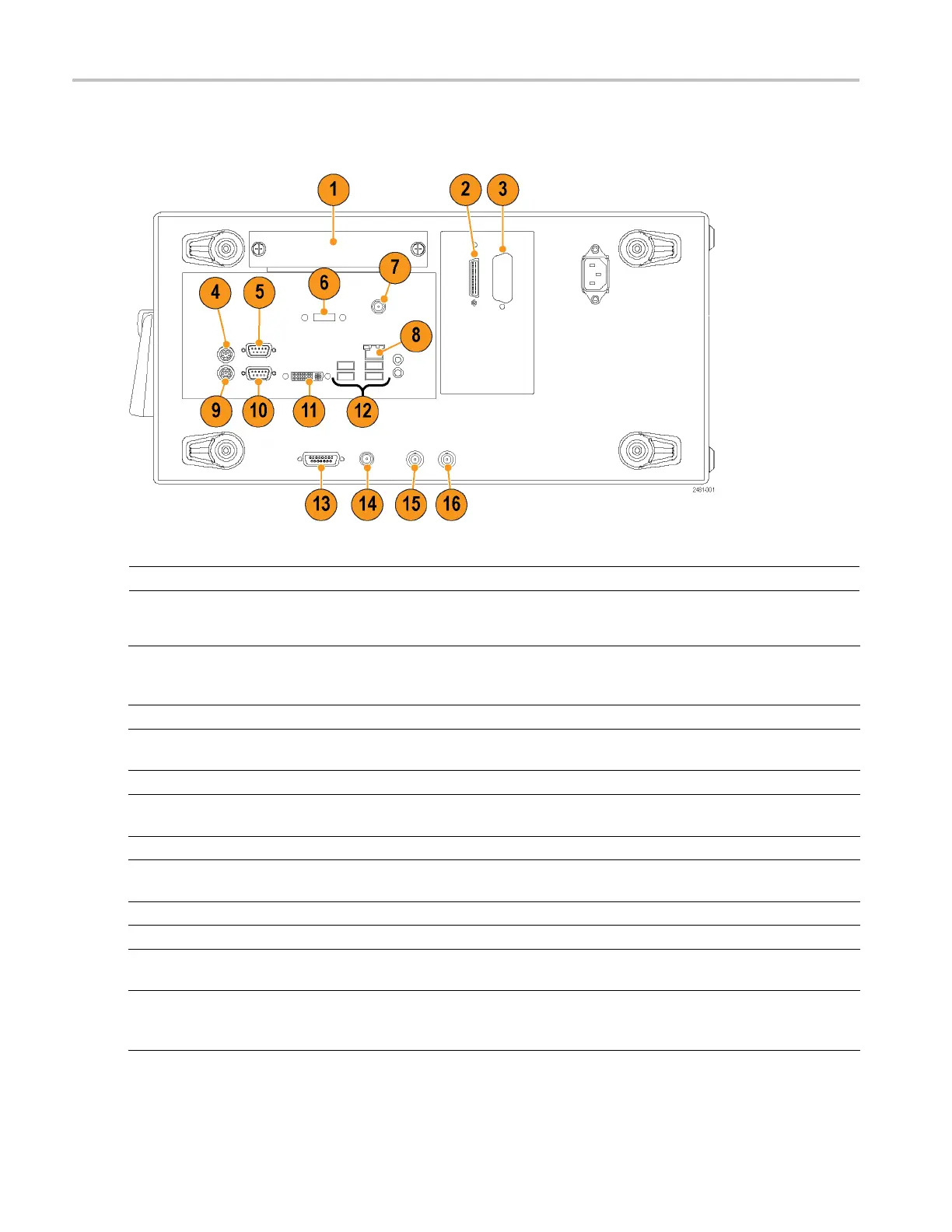
Rear Panel (AWG7
000C Series)
Rear Panel (AW
G7000C Series)
NOTE. AWG7000B series have a similar connectors in different locations.
Connector Description
1. Removable HDD
Removable hard disk drive to secure data. If you remove the HDD, user
information such as setup files or waveform data does not remain within
the instrument.
2. TekLink
Use the TekLink connector for data import.
3. GPIB Use the GPIB connector to connect the instrument to a GPIB controller
for GPIB operation.
4. PS-2 Mouse connector Use the PS-2 connector to connect a mouse to the instrument.
5. COM2 Use the COM2 serial port to connect to other devices through the serial
port.
6. eSATA port U se the eSATA port to connect external SATA devices to the instrument.
7. Synchronization Clock Ou t port Use the Synchronization Clock Out port to provide a synchronization signal
to other external devices. Terminate this connector w hen not in use.
8. LAN Use the RJ-45 connector to connect the instrument to a network.
9. PS-2 K eyboard connector Use the PS-2 connector to c onnect a PS-2 keyboard to the instrument.
10. COM1 Use the COM1 serial port to connect to other devices through the serial
port.
11. Video
Use the DVI-I Video port to connect a monitor for extended desktop
operation. To connect a VGA monitor to the DVI-I connector, use a
VGA-to-DVI adapter.
14 AWG5000 and AWG7000 Series Quick Start User Manual
 Loading...