ME910G1 HW Design Guide
1VV0301593 Rev.7 Page 73 of 98 2021-02-02
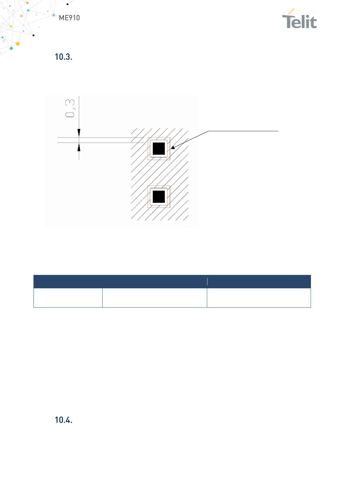
Recommendations for PCB pad dimensions
It is not recommended to place via or micro-via not covered by solder resist in an area of
0,3 mm around the pads unless it carries the same signal of the pad itself
Figure 29: Pad dimensions recommendations
Holes in pad are allowed only for blind holes and not for through holes.
Recommendations for PCB pad surfaces:
Electro-less Ni /
Immersion Au
good solder ability protection,
high shear force values
Table 33: Recommendations for PCB pad surfaces
The PCB must be able to resist the higher temperatures that occur during the lead-free
process. This issue should be discussed with the PCB-supplier. Generally, the wettability
of tin-lead solder paste on the described surface plating is better compared to the lead-
free solder paste.
It is not necessary to panel the application’s PCB, however in that case it is recommended
to use milled contours and predrilled board breakouts; scoring or v-cut solutions are not
recommended.
Thermal performance
FR4 is one of the most commonly used PCB materials, it is a flame retardant composite
material, composed by fiberglass-reinforced and epoxy laminate. One of the features of
the FR4, is to have a very low thermal conductivity. An inexpensive way to improve thermal
Inhibit area for micro-via
 Loading...