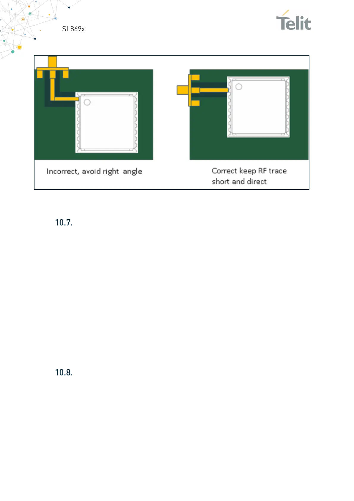
Figure 23: RF Trace Examples
PCB Stack and Trace Impedance
It is important to maintain a 50 Ω impedance on the RF path trace. Design software for
calculating trace impedance can be found from multiple sources on the internet. The best
method is to contact your PCB supplier and request a stackup for a 50 Ω controlled
impedance board. They will give you a suggested trace width along with PCB stackup
needed to create the specified impedance.
It is also important to consider the effects of component pads that are in the path of the
50 Ω trace. If the traces are shorter than a 1/16th wavelength, transmission line effects
will be minimized, but stray capacitance from large component pads can induce
additional RF losses. It may be necessary to ask the PCB vendor to generate a new PCB
stackup and suggested trace width that is closer to the component pads, or modify the
component pads themselves.
Input to the Pre-select SAW Filter (SL869-V2 and SL869-
V2S only)
The SL869-V2 and SL869-V2S modules include a pre-select SAW filter at the RF input in
front of the internal LNA. Thus, the RF input of the module is connected directly to the
SAW filter. Any circuit connected to the RF input pin would see a complex impedance
presented by the SAW filter (especially out of band), rather than the relatively broad and
flat return loss presented by an LNA. Filter devices pass the desired in-band signal,
 Loading...