SL869x-V2 Family Product User Guide
1VV0301175 Rev. 9 Page 65 of 93 2021-07-15
11. REFERENCE DESIGNS
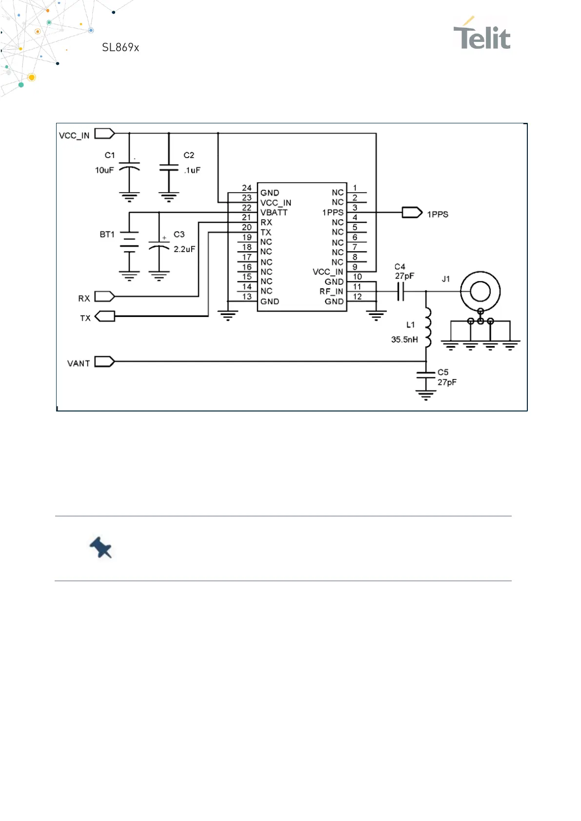
Figure 24: SL869-V2 Family Reference Design
Along with power and grounds, the minimum signals required to operate the receiver
properly are the RF input signal and two digital signals (TX and RX). The RF input can be
connected directly to a passive GNSS antenna. The reference design shows a DC power
feed for an active antenna.
Note: C4 is used to block the DC voltage from entering the module
but is not required on SL869L-V2 modules since they include an
internal DC blocking capacitor.
Inductor L1 is chosen to be self-resonant at the GNSS frequency (approximately 1.57542
GHz) to minimize loading on the RF trace. Capacitor C5 is chosen to be self-resonant so
that it is close to an RF short at the GNSS frequency.
The circuit above does not provide input to ANT-OC and ANT-SC-N (SL869-V2 only).
Please refer to the schematic below.
TX and RX are UART lines with a default of 9600-8-N-1. They are used for message output
and command input. Be careful not to drive the RX line if the module is turned off.
Refer to the tables in chapter 9 Electrical Interface for details.
 Loading...