WE310G4-I/P Module Hardware User Guide
1VV0301767 Rev. 5 Page 33 of 48 2022-11-08
Not Subject to NDA
PCB Pad Dimensions
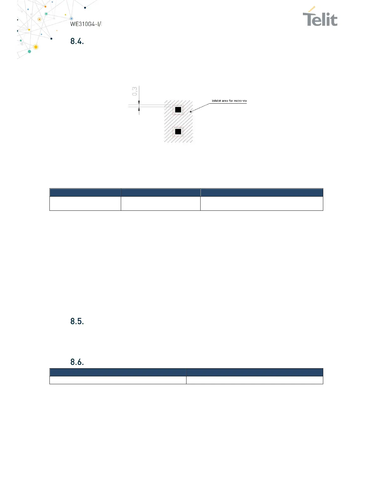
It is not recommended to place via or micro-via not covered by the solder resist in an
area of 0.3 mm around the pads unless it carries the same signal of the pad itself as
shown below.
Figure 22: Inhibit Area for Not Solder Covered Vias
The holes in the pad are allowed only for blind holes and not for through holes. The
following table shows the recommended PCB pad surfaces.
Finish Layer thickness [µm] Properties
Electro-less Ni /
Immersion Au
3 –7 / 0.03 – 0.15 Good solderability protection,
high shear force values
Table 17: PCB Finishing Recommendation
The PCB must be able to resist the higher temperatures which can occur during the
lead-free process. This issue should be discussed with the PCB supplier. Generally, the
wettability of tin-lead solder paste on the described surface plating is better compared
to lead-free solder paste.
It is not necessary to panel the application PCB. However, it is recommended to use
milled contours and predrilled board breakouts; scoring or v-cut solutions are NOT
recommended.
Stencil
The Stencil’s aperture layout can be the same as the recommended footprint (1:1). It is
recommended to use a stencil foil with a thickness
≥
120 µm.
Solder Paste
Component Lead-free
Solder paste Sn/Ag/Cu
Table 18: Recommended Solder Paste Type
To avoid or minimize the cleaning efforts after assembly, it is recommended to use a
“no-clean” solder paste.
 Loading...