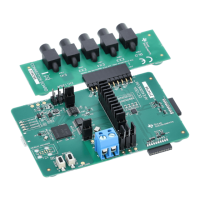
EVM Overview
www.ti.com
6
SBAU090E–November 2003–Revised November 2018
Submit Documentation Feedback
Copyright © 2003–2018, Texas Instruments Incorporated
ADS1256EVM and ADS1256EVM-PDK
The power connector (J3) carries the power supplies. The ADS1256EVM requires a +5V analog supply
and a +1.8V to +3.3V digital supply. The board is designed using a single ground net connected to DGND.
An AGND pin is also provided. Power options are routed through J4, J9, and J10.
The GPIO header (J5) provides a connection to the four GPIO pins on the EVM.
The ADS1256 uses separate supplies for its analog and digital sections. A jumper is inserted in each
supply line. These jumpers allow the current of each supply to be measured independently.
1.5 Controls
The ADS1256EVM is configured using four slide switches and a jumper.
Switches S1 and S2 select the input signal provided to the first four multiplexer inputs on the ADS1256.
Normally you will use the external input, but you can also use the switches to short the inputs together and
to connect the reference voltage to the inputs. Additionally, the latter two positions are useful for
conducting noise and functional tests.
Switch S3 selects the reference input. One position selects the external reference input pins on the analog
connector (J1). The other two positions connect the onboard +2.5V reference in one of two ways: between
ground and the reference, or between the reference and the analog supply.
Switch S4 selects the system clock source for the ADS1256. You can select between the onboard
7.68MHz crystal or an external clock.
All switches and their settings are additionally described in later sections of this user guide.
2 Analog Interface
For maximum flexibility, the ADS1256EVM is designed for easy interfacing to multiple analog sources.
Samtec part numbers SSW-110-22-F-D-VS-K and TSM-110-01-T-DV-P provide a convenient 10-pin, dual-
row, header/socket combination at J1. This header/socket provides access to the analog input pins of the
ADS1256. Consult Samtec at www.samtec.com or call 1-800-SAMTEC-9 for a variety of mating connector
options.
Most of the pins on J1 are directly connected, with minimal filtering or protection. Use appropriate caution
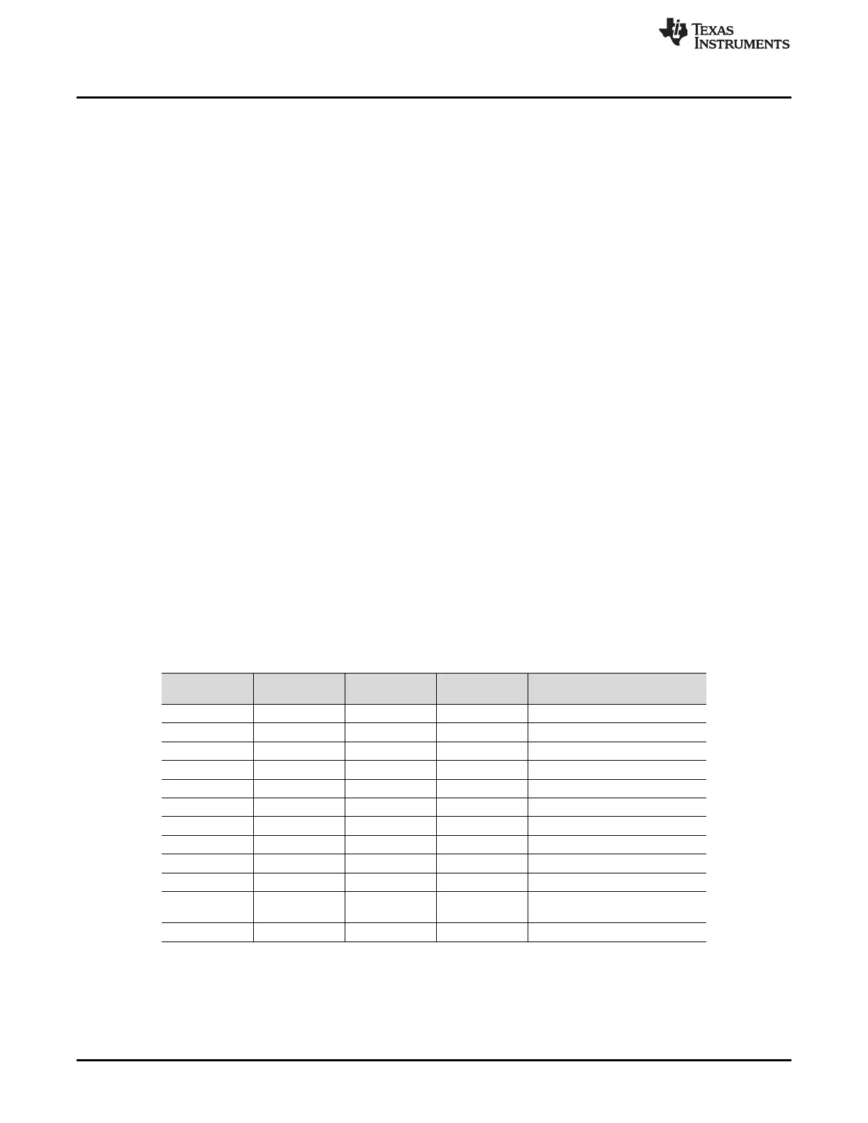
when handling these pins. Table 1 summarizes the pinout for analog interface J1.
Table 1. J1: Analog Interface Pinout
Pin Number Pin Name
Standard
Name Direction Function
J1.1 AIN0 AN0– Input Analog input 1 (switched by S1)
J1.2 AIN1 AN0+ Input Analog input 0 (switched by S1)
J1.3 AIN2 AN1– Input Analog input 3 (switched by S1)
J1.4 AIN3 AN1+ Input Analog input 2 (switched by S1)
J1.5 AIN4 AN2– Input Analog input 4
J1.6 AIN5 AN2+ Input Analog input 5
J1.7 AIN6 AN3– Input Analog input 6
J1.8 AIN7 AN3+ Input Analog input 7
J1.10 AINCOM AN4+ Input Analog input common
J1.18 SYSREFN REF– Input Inverting external reference input
J1.20 SYSREFP REF+ Input Noninverting external reference
input
J1.9-J1.19 odd GND AGND Input Signal ground