www.ti.com
Digital Interface
7
SBAU090E–November 2003–Revised November 2018
Submit Documentation Feedback
Copyright © 2003–2018, Texas Instruments Incorporated
ADS1256EVM and ADS1256EVM-PDK
3 Digital Interface
3.1 Serial Data Interface
The ADS1256EVM is designed to easily interface with multiple control platforms. Samtec part numbers
SSW-110-22-F-D-VS-K and TSM-110-01-T-DV-P provide a convenient 10-pin, dual-row, header/socket
combination at J2. This header/socket provides access to the digital control and serial data pins of the
TSC. Consult Samtec at www.samtec.com or call 1-800-SAMTEC-9 for a variety of mating connector
options.
All logic levels on J2 are 3.3V CMOS, except for the I
2
C pins, which conform to 3.3V I
2
C rules.
Some pins on J2 have weak pullup resistors. These resistors provide default settings for many of the
control pins. Most pins on J2 correspond directly to ADS1256 pins. See the ADS1256 product data sheet
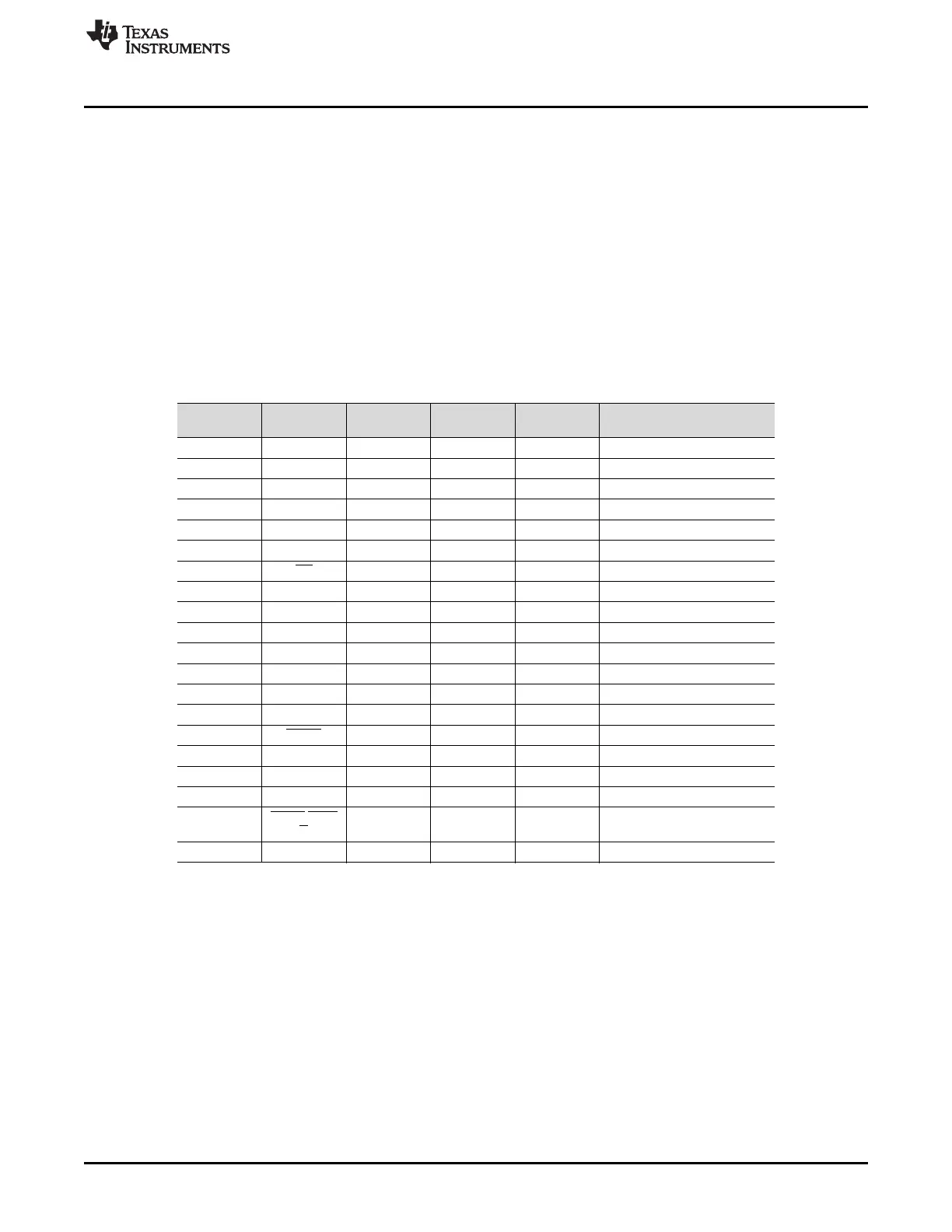
for complete details on these pins. Table 2 describes the J2 serial interface pins.
Table 2. J2: Serial Interface Pins
Pin Number Pin Name
Standard
Name Direction Pulldown Function
J2.1 — CNTL — None Unused
J2.2 — GPIO0 — None Unused
J2.3 SCLK CLKX Input None Serial clock input
J2.4 DGND DGND I/O Power Digital ground
J2.5 — CLKR — None Unused
J2.6 — GPIO1 — None Unused
J2.7 CS FSX Input None Chip select (via J8)
J2.8 — GPIO2 — None Unused
J2.9 — FSR — None Unused
J2.10 DGND DGND I/O Power Digital ground
J2.11 DIN DX Input None Serial data input
J2.12 — GPIO3 — None Unused
J2.13 DOUT DR Input None Serial data output
J2.14 RESET GPIO4 Input Yes Reset input (via J7)
J2.15 DRDY INT Output None Data ready signal
J2.16 SCL SCL I/O None I
2
C clock line
J2.17 EXTCLK TOUT Input None External system clock input
J2.18 DGND DGND I/O Power Digital lround
J2.19 SYNC/PDW
N
GPIO5 Input Yes Synchronization and power
down control pin (via J6)
J2.20 SDA SDA I/O None I
2
C data line
3.2 GPIO
The ADS1256 has four general-purpose I/O (GPIO) pins. One of these pins can also be configured as a
buffered system clock output. This output is typically used to clock additional ADS1255/ADS1256 devices,
but can be used for other purposes as well. The GPIO pins for the ADS1256 are shown in Figure 2. These
pins (from left to right) are D3 to D0.