KCU105 Board User Guide www.xilinx.com 46
UG917 (v1.4) September 25, 2015
Chapter 1: KCU105 Evaluation Board Features
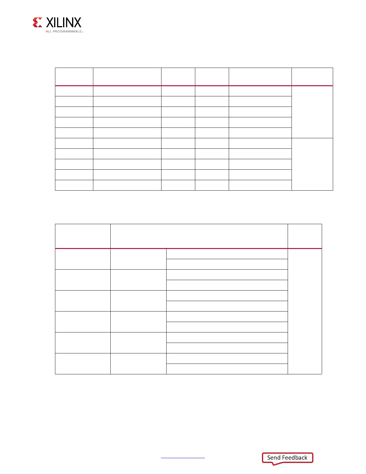
Tab le 1- 13 lists the SFP+ module connections to FPGA U1.
Table 1-13: KCU105 Board FPGA U1 to SFP0 and SFP1 Module Connections
FPGA (U1)
Pin
Schematic Net Name
FPGA (U1)
Direction
Pin
Number
Pin Name
SFP/SFP+
Module
T2 SFP0_RX_P Input 13 RD_P
SFP0 P5
T1 SFP0_RX_N Input 12 RD_N
U4 SFP0_TX_P Output 18 TD_P
U3 SFP0_TX_N Output 19 TD_N
AL8 SFP0_TX_DISABLE Output 3 TX_DISABLE
V2 SFP1_RX_P Input 13 RD_P
SFP1 P4
V1 SFP1_RX_N Input 12 RD_N
W4 SFP1_TX_P Output 18 TD_P
W3 SFP1_TX_N Output 19 TD_N
AM9 SFP1_TX_DISABLE Output 3 TX_DISABLE
Notes:
1. SFP0_TX_DISABLE, SFP1_TX_DISABLE I/O standard LVCMOS18; MGT connections I/O standard not applicable.
Table 1-14: SFP0 and SFP1 Module Control and Status Connections
SFP Control/Status
Signal
Board Connection
SFP
Module
SFP_TX_FAULT Test Point J16
High = Fault
SFP0 P5
Low = Normal operation
SFP_TX_DISABLE Jumper J6
Off = SFP Disabled
On = SFP Enabled
SFP_MOD_DETECT Test Point J17
High = Module not present
Low = Module present
SFP_RS0 Jumper J42
Jumper pins 1-2 = Full RX bandwidth
Jumper pins 2-3 = Reduced RX bandwidth
SFP_RS1 Jumper J41
Jumper pins 1-2 = Full RX bandwidth
Jumper pins 2-3 = Reduced RX bandwidth
SFP_LOS Test Point J18
High = Loss of receiver signal
Low = Normal operation