KCU105 Board User Guide www.xilinx.com 43
UG917 (v1.4) September 25, 2015
Chapter 1: KCU105 Evaluation Board Features
PCI Express Endpoint Connectivity
[Figure 1-2, callout 14]
The 8-lane PCI Express edge connector P1 performs data transfers at the rate of 2.5 GT/s for
Gen1 applications, 5.0 GT/s for Gen2 applications, and 8.0 GT/s for Gen3 applications. The
PCIe transmit and receive signal datapaths have a characteristic impedance of 85Ω ± 10%.
The PCIe clock is routed as a 100Ω differential pair.
The PCIe transmit and receive signal data paths are routed with a differential characteristic
impedance of 85Ω (±10%) with an insertion loss of <4 dB up to 8 GHz.
The XCKU040-2FFVA1156E (-2 speed grade) device included with the KCU105 board
supports up to Gen3 x8.
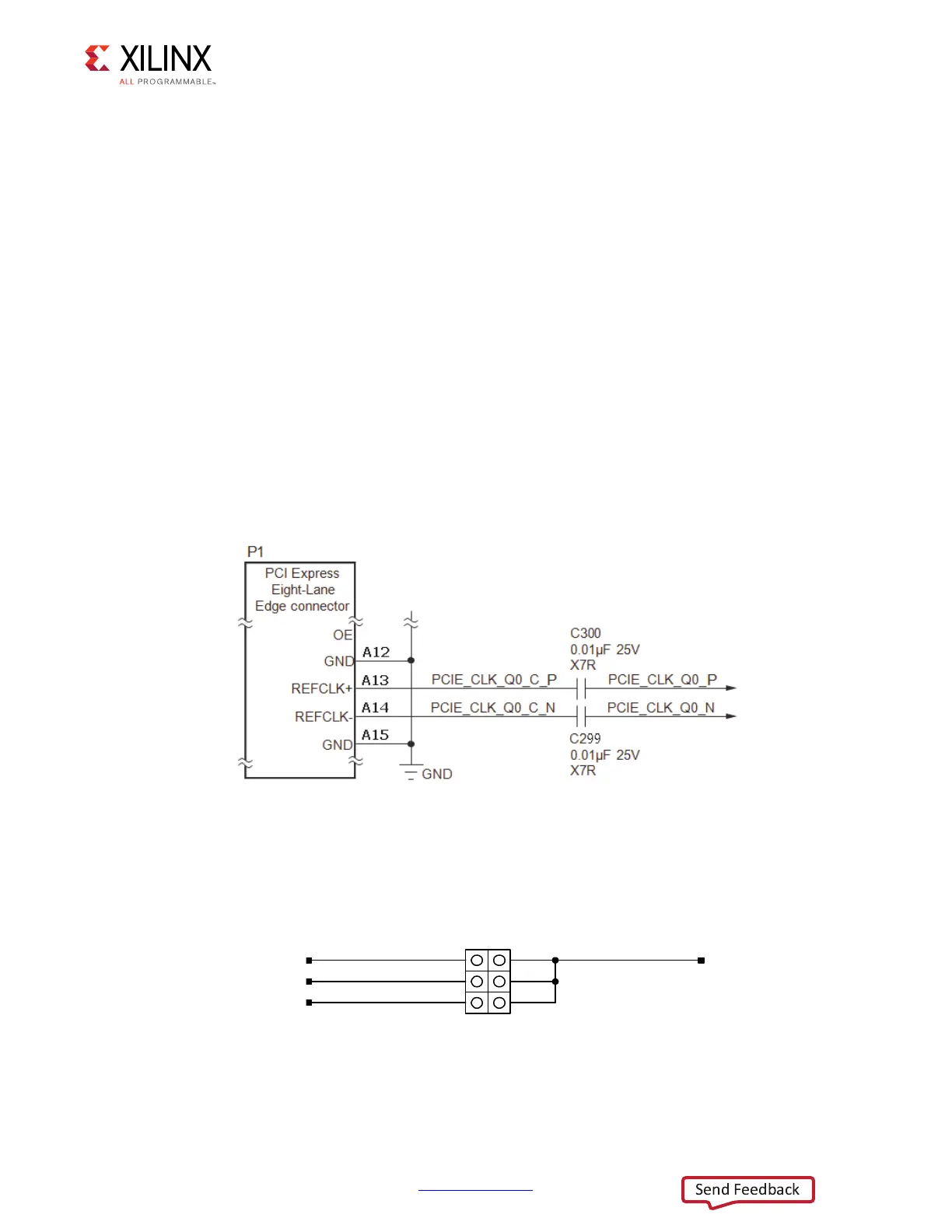
The PCIe reference clock input is from the P1 edge connector. It is AC coupled to FPGA U1
through the MGTREFCLK0 pins of Quad 225. PCIE_CLK_Q0_P is connected to U1 pin AB6,
and the _N net is connected to pin AB5. The PCI Express clock circuit is shown in
Figure 1-16.
PCIe lane width/size is selected by jumper J74 (Figure 1-17). The default lane size selection
is 8-lane (J74 pins 5 and 6 jumpered).
X-Ref Target - Figure 1-16
Figure 1-16: PCI Express Clock
X-Ref Target - Figure 1-17
Figure 1-17: PCI Express Lane Size Select Jumper J74
-
+'5B;
3&,(B35617B;
3&,(B35617B;
3&,(B35617B; 3&,(B35617B%
8*BB