KCU105 Board User Guide www.xilinx.com 17
UG917 (v1.4) September 25, 2015
Chapter 1: KCU105 Evaluation Board Features
DDR4 Component Memory
[Figure 1-2, callout 2]
The 2 GB DDR4 component memory system is comprised of four 256 Mb x 16 DDR4 SDRAM
devices (Micron EDY4016AABG-DR-F-D) located at U60-U63. This memory system is
connected to the XCKU040 HP banks 44, 45, and 46. The DDR4 0.6V VTT termination voltage
(net DDR4_VTT) is sourced from the TI TPS51200DR linear regulator U24. The connections
between the DDR4 component memories and the XCKU040 banks 44, 45, and 46 are listed
in Tab le 1-4.
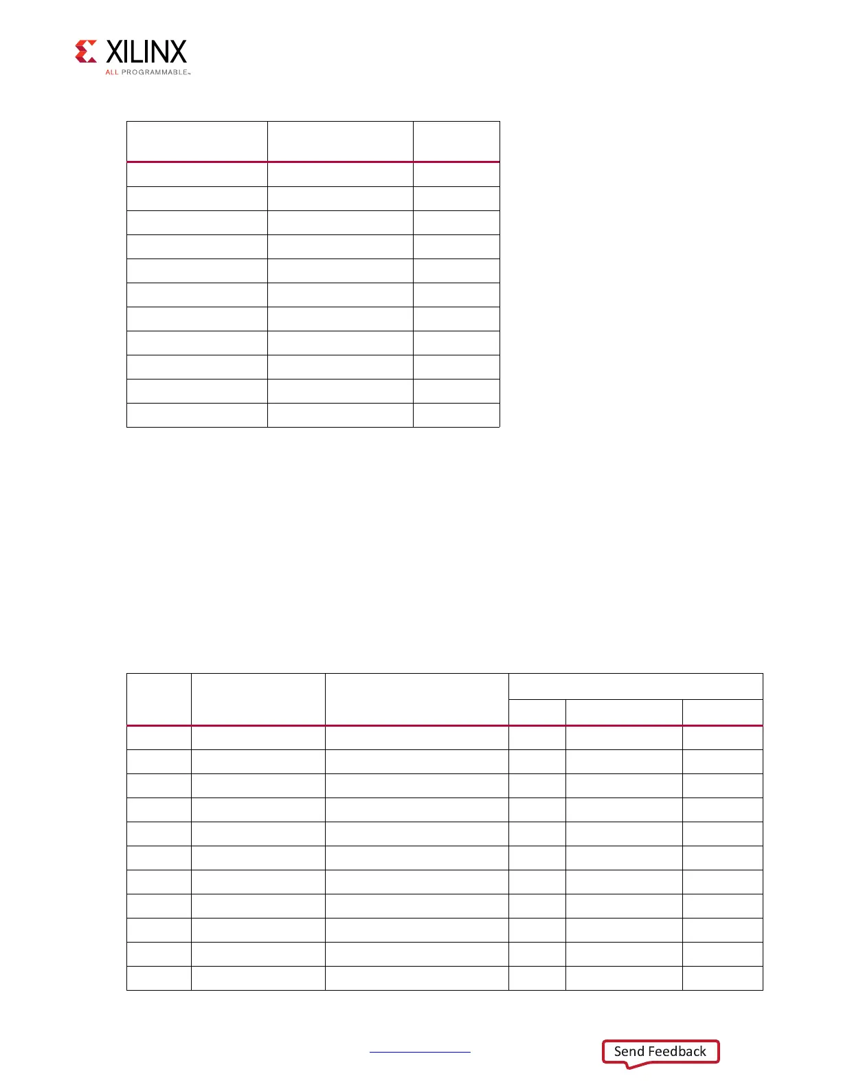
Table 1-3: I/O Bank Voltage Rails
FPGA (U1) Bank
Power Supply Rail
Net Name
Voltage
Bank 0 VCC1V8_FPGA 1.8V
HP Bank 44 VCC1V2_FPGA 1.2V
HP Bank 45 VCC1V2_FPGA 1.2V
HP Bank 46 VCC1V2_FPGA 1.2V
HP Bank 47 VADJ_1V8_FPGA 1.8V
HP Bank 48 VADJ_1V8_FPGA 1.8V
HR Bank 64 VCC1V8_FPGA 1.8V
HR Bank 65 VCC1V8_FPGA 1.8V
HP Bank 66 VADJ_1V8_FPGA 1.8V
HP Bank 67 VADJ_1V8_FPGA 1.8V
HP Bank 68 VADJ_1V8_FPGA 1.8V
Table 1-4: DDR4 Memory Connections to the FPGA
FPGA
(U1) Pin
Schematic Net
Name
I/O Standard
Component Memory
Pin # Pin Name Ref. Des.
AE23 DDR4_DQ0 POD12_DCI G2 DQL0 U60
AG20 DDR4_DQ1 POD12_DCI F7 DQL1 U60
AF22 DDR4_DQ2 POD12_DCI H3 DQL2 U60
AF20 DDR4_DQ3 POD12_DCI H7 DQL3 U60
AE22 DDR4_DQ4 POD12_DCI H2 DQL4 U60
AD20 DDR4_DQ5 POD12_DCI H8 DQL5 U60
AG22 DDR4_DQ6 POD12_DCI J3 DQL6 U60
AE20 DDR4_DQ7 POD12_DCI J7 DQL7 U60
AJ24 DDR4_DQ8 POD12_DCI A3 DQU0 U60
AG24 DDR4_DQ9 POD12_DCI B8 DQU1 U60
AJ23 DDR4_DQ10 POD12_DCI C3 DQU2 U60