EasyManuals Logo

Xilinx KCU105 User Manual

Xilinx KCU105
143 pages
To Next Page IconTo Next Page
To Previous Page IconTo Previous Page
Page #16 background imageLoading...
Page #16 background image
KCU105 Board User Guide www.xilinx.com 16
UG917 (v1.4) September 25, 2015
Chapter 1: KCU105 Evaluation Board Features
I/O Voltage Rails
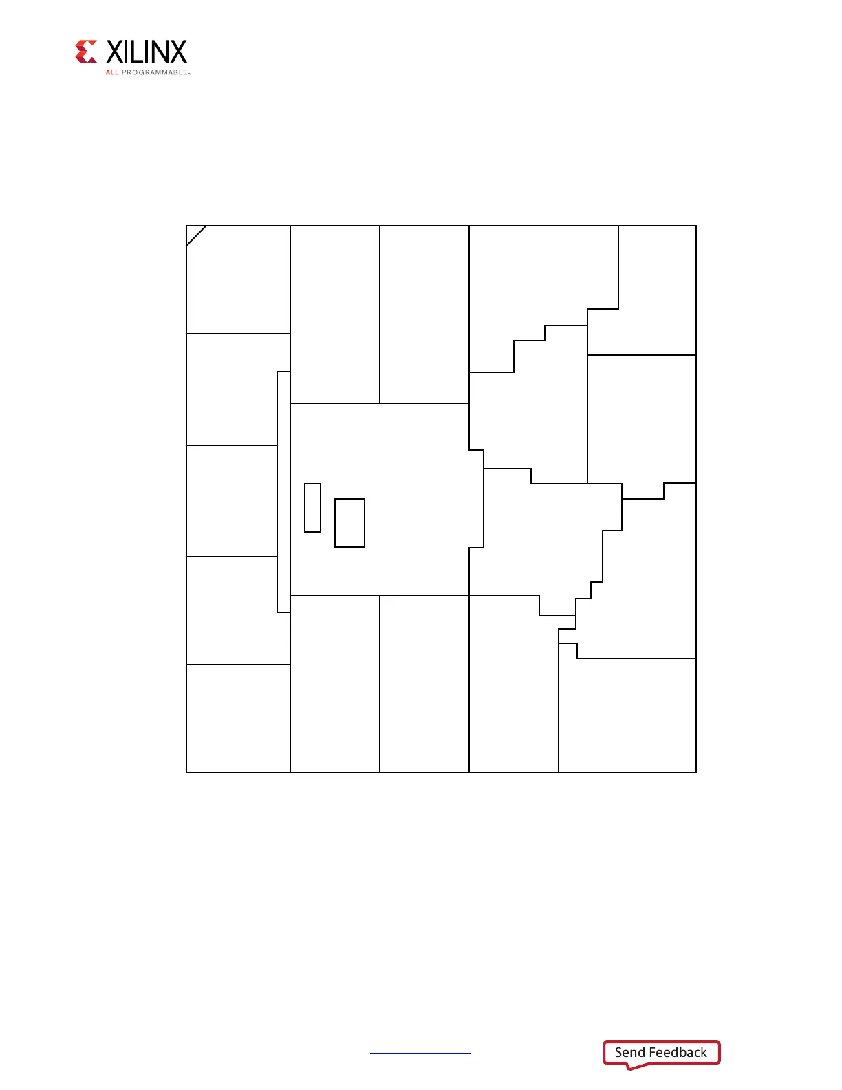
There are ten I/O banks available on the KCU040 device and the KCU105 board. The
voltages applied to the FPGA I/O banks (shown in Figure 1-5) used by the KCU105 board are
listed in Tabl e 1-3.
X-Ref Target - Figure 1-5
Figure 1-5: UltraScale XCKU040 Bank Locations
*7+

*7+

*7+

*7+

*7+


+5

+3

+3

+3

+3

+3

+5

+3
1RWXVHG

+3

+3
9&&,17
9&&$8;
[FNXIIYD
&RUH3RZHU
8*BB
1RWXVHG
Send Feedback

Table of Contents

Other manuals for Xilinx KCU105

Questions and Answers:

Question and Answer IconNeed help?

Do you have a question about the Xilinx KCU105 and is the answer not in the manual?

Xilinx KCU105 Specifications

General IconGeneral
BrandXilinx
ModelKCU105
CategoryMotherboard
LanguageEnglish

Related product manuals