KCU105 Board User Guide www.xilinx.com 21
UG917 (v1.4) September 25, 2015
Chapter 1: KCU105 Evaluation Board Features
The KCU105 board DDR4 memory component interface adheres to the constraints
guidelines documented in the DDR4 Design Guidelines section of UltraScale Architecture
PCB Design User Guide (UG583) [Ref 17] and in UltraScale Architecture-Based FPGAs
Memory Interface Solutions LogiCORE IP Product Guide (PG150) [Ref 4]. The KCU105 board
DDR4 memory component interface is a 40Ω impedance implementation. For more details
about the Micron DDR4 component memory, see the Micron EDY4016AABG-DR-F-D data
sheet at the Micron website [Ref 22].
Dual Quad-SPI Flash Memory
[Figure 1-2, callout 3]
The Quad-SPI flash memory located at U35 and U36 provides 2 x 256 Mb of nonvolatile
storage that can be used for configuration and data storage. For details on FPGA
configuration operation and implementation related to the dual Quad-SPI interfaces, see
UltraScale Architecture Configuration User Guide (UG570) [Ref 3].
• Part number: N25Q256A11ESF40F (Micron)
•Supply voltage: 1.8V
• Datapath width: 4 bits
• Data rate: various depending on single/dual/quad mode
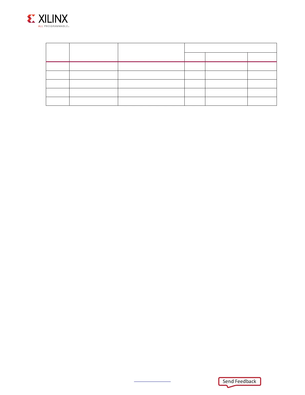
AL19 DDR4_CS_B SSTL12_DCI L7 CS_B U60-U62
AD15 DDR4_CKE SSTL12_DCI K2 CKE U60-U62
AL18 DDR4_RESET_B LVCMOS12 P1 RESET_B U60-U62
AE16 DDR4_CK_T DIFF_SSTL12_DCI K7 CK_T U60-U62
AE15 DDR4_CK_C DIFF_SSTL12_DCI K8 CK_C U60-U62
Table 1-4: DDR4 Memory Connections to the FPGA (Cont’d)
FPGA
(U1) Pin
Schematic Net
Name
I/O Standard
Component Memory
Pin # Pin Name Ref. Des.