KCU105 Board User Guide www.xilinx.com 22
UG917 (v1.4) September 25, 2015
Chapter 1: KCU105 Evaluation Board Features
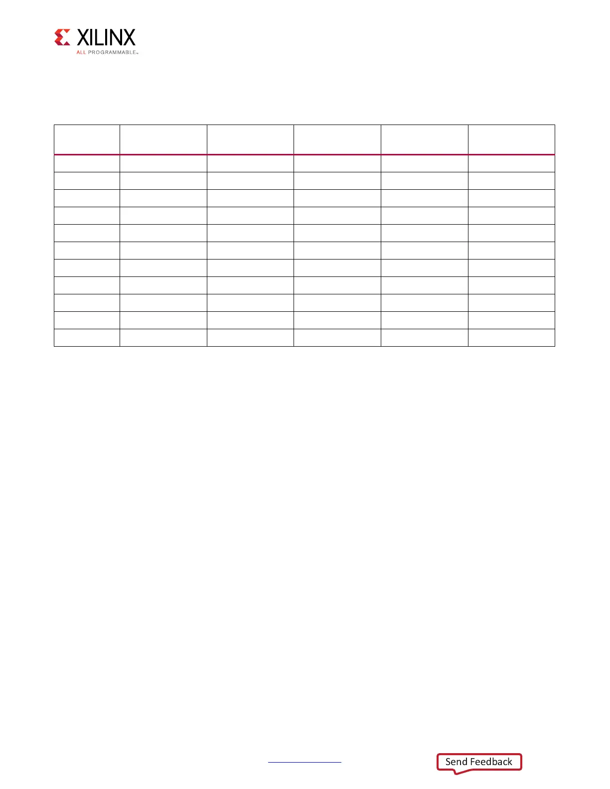
The connections between the SPI flash memories and the XCKU040 device are listed in
Tab le 1- 5.
Figure 1-6 shows the connections of the linear Quad-SPI flash memory on the KCU105
evaluation board. For more details, see the Micron N25Q256A11ESF40F data sheet at the
Micron website [Ref 22].
Table 1-5: Quad-SPI Flash Memory Connections to FPGA U1
FPGA (U1)
Pin
Schematic Net
Name
I/O Standard Pin # Pin Name Ref. Des.
AC7 QSPI0_IO0 LVCMOS18 15 SI_IO0 U35
AB7 QSPI0_IO1 LVCMOS18 8 SI_IO1 U35
AA7 QSPI0_IO2 LVCMOS18 9 SI_IO2 U35
Y7 QSPI0_IO3 LVCMOS18 1 SI_IO3 U35
AA9 FPGA_CCLK NA
(1)
16 SCK U35, U36
U7 QSPI0_CSB LVCMOS18 7 CS_B U35
M20 QSPI1_IO0 LVCMOS18 15 SI_IO0 U36
L20 QSPI1_IO1 LVCMOS18 8 SI_IO1 U36
R21 QSPI1_IO2 LVCMOS18 9 SI_IO2 U36
R22 QSPI1_IO3 LVCMOS18 1 SI_IO3 U36
G26 QSPI1_CSB LVCMOS18 7 CS_B U36
Notes:
1. CCLK is a dedicated pin and does not require an IOSTANDARD or LOC attribute.