KCU105 Board User Guide www.xilinx.com 55
UG917 (v1.4) September 25, 2015
Chapter 1: KCU105 Evaluation Board Features
I2C Bus, Topology, and Switches
[Figure 1-2, callouts 21, 22]
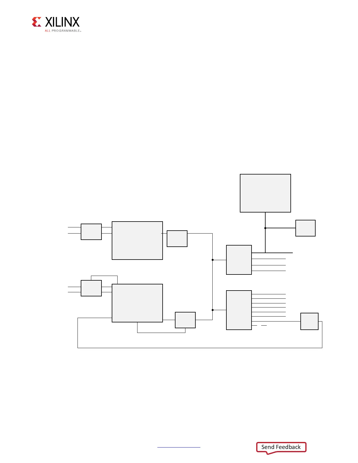
The KCU105 evaluation board implements a 2-to-1 I2C bus arrangement. A single I2C bus
from the FPGA U1 XCKU040 (IIC_MAIN_SCL/SDA_LS) and system controller Zynq-7000 AP
SoC U111 (SYSCTLR_I2C_SCL/SDA) is wired to the main I2C bus via level-shifters. FPGA U1 is
wired through level-shifter U77 and system controller U111 is wired through level-shifter
U108. The output sides of U77 and U108 are wired in parallel to the main I2C bus (IIC_SDA
and _SCL_MAIN). This common main I2C bus is then routed to a pair of bus switches, a TI
TCA9548 1-to-8 channel I2C bus switch (U28) and a TI PCA9544 1-to-4 channel I2C bus
switch (U80). The bus switches can operate at speeds up to 400 kHz.
The KCU105 evaluation board I2C bus topology overview is shown in Figure 1-23 and
Tab le 1- 19 lists the address for each device on the I2C bus.
Note:
See Table 1-19 for device I2C address assignments.
X-Ref Target - Figure 1-23
Figure 1-23: I2C Bus Topology Overview
,,&08;
,,&08;
0$;,0SRZHU
UHJXODWRUV
)3*$
6<6&RQWUROOHU
6<6B9
,,&
87,/B9WR6<6B9
6<6B9WR87,/B9
0$;,0B&$%/(B%
30%86B$/(57
87,/B9WR9&&9B$
0$;,0B&$%/(B%
30%86B$/(57
9&&9B$
6<6021B'&
9&&9B$WR87,/B9
87/B9
87/B9
[
[
87,/B9WR6<6B9
,,&B0$,1
9B6:
;±[
'21(B%8)
'21(B%8)
6<6021,,&
;
Y
30%86
)0&+3&
)0&/3&
((3520
6,[
3RUW([SDQGHU
6)3
6)3
6,
$'9+'0,
6<6021B,,&
1&
30%866'$
6&/
/HYHO
VKLIWHU
DOZD\V
HQDEOHG
/HYHO
VKLIWHU
DOZD\V
HQDEOHG
/HYHO
VKLIWHU
Z2(
/HYHO
VKLIWHU
Z2(
0$;,0
&DEOH
/HYHO
VKLIWHU
DOZD\V
HQDEOHG
8*BB
7&$
3&$