VC707 Evaluation Board www.xilinx.com 57
UG885 (v1.4) May 12, 2014
Feature Descriptions
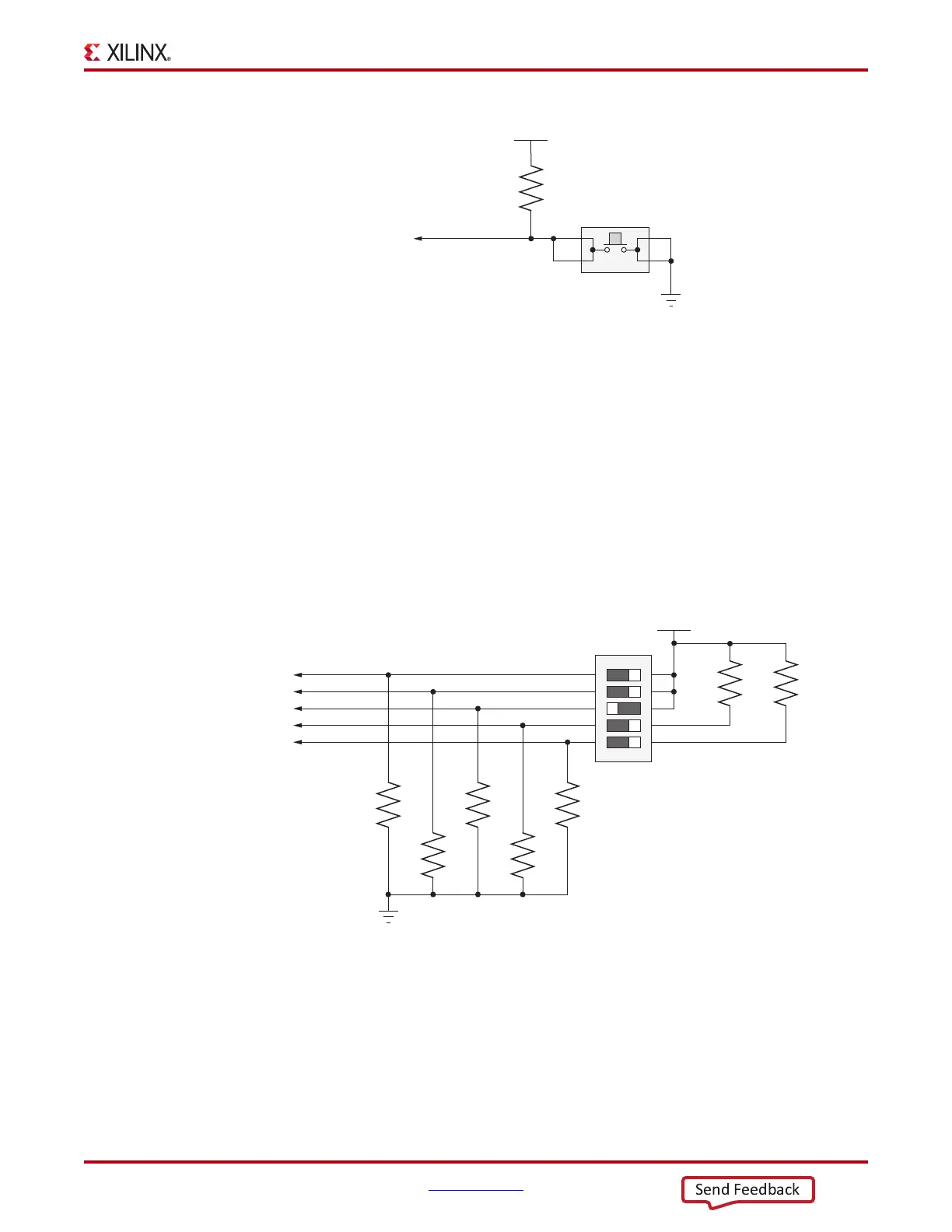
Configuration Mode and Upper Linear Flash Address Switch (SW11)
[Figure 1-2, callout 29]
FPGA Configuration Mode: DIP switch SW11 positions 3, 4, and 5 control which
configuration mode is used at power-up or when the PROG pushbutton is pressed.
Linear BPI Flash Upper Addresses: DIP switch SW11 positions 1 and 2 control the setting
of address bits FLASH_A25 and FLASH_A24. The mode signals FPGA_M2, _M1 and _M0
are connected to FPGA U1 pins AJ10, AK10 and AL10 respectively. Configuration mode is
used at power-up or when the PROG pushbutton is pressed.
Figure 1-32 shows the SW11 circuit.
X-Ref Target - Figure 1-31
Figure 1-31: FPGA_PROG_B Pushbutton SW9
UG885_c1_28_030512
VCC1V9
FPGA_PROG_B
R42
4.7kΩ
0.1 W
5%
GND
1
23
4
SW9
X-Ref Target - Figure 1-32
Figure 1-32: Configuration Mode and Upper Linear Flash Address Switch
UG885_c1_29_030512
SDA05H1SBD
SW11
R226
220Ω
0.1 W
1%
R227
220Ω
0.1 W
1%
VCC1V8
FPGA_M2
FPGA_M1
FPGA_M0
FLASH_A25
FLASH_A24
R341
1.21kΩ
0.1 W
1%
R340
1.21kΩ
0.1 W
1%
R339
1.21kΩ
0.1 W
1%
R338
1.21kΩ
0.1 W
1%
R337
1.21kΩ
0.1 W
1%
1
2
3
4
5
10
9
8
7
6
GND