Virtex-6 FPGA Connectivity Kit Getting Started www.xilinx.com 43
UG664 (v1.4) July 6, 2011
Modifying the Virtex-6 FPGA Targeted Reference Design
d. After successful implementation of the design, a results folder with these FPGA
programming files is generated:
- FPGA programming bit file: <filename>.bit (in this case, it is
v6_pcie_10Gdma_ddr3_xaui.bit)
- SPI x4 flash programming MCS file: <filename>.mcs (in this case, it is
ML605.mcs)
6. Program the FPGA:
a. If the ML605 board is still plugged into the PC system, shut down the PC system
and remove the ML605 board.
b. To program the FPGA using Platform Flash, refer to the jumper settings detailed in
step 4 of Hardware Demonstration Setup Instructions, page 12.
c. For all other ML605 switch and jumper settings, keep them at the factory default
configuration as indicated in UG534
, ML605 Hardware User Guide.
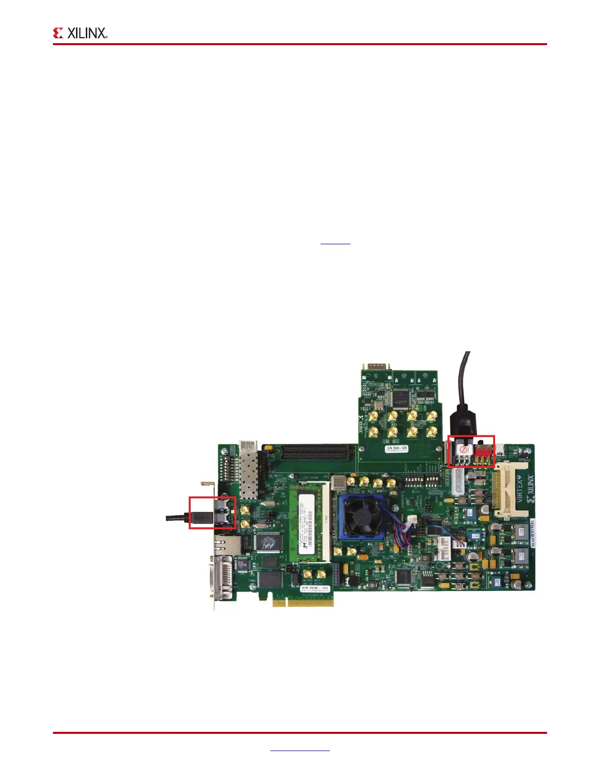
7. Set up the board:
a. Connect the mini USB cable to the USB-JTAG connector as shown in Figure 36. The
other end of the USB cable is connected to the PC system or laptop on which the
Xilinx design tools were installed.
b. Power off the ML605 board (the power switch should be towards the bracket
edge). Use the included wall power adapter to provide 12V power to the 6-pin
connector. Power on the ML605 board.
X-Ref Target - Figure 36
Figure 36: Setting Up the Board

 Loading...

