EasyManua.ls Logo

Yamaha DG-Stomp Service Manual

Yamaha DG-Stomp
42 pages
To Next Page IconTo Next Page
Page #1 background imageLoading...
Page #1 background image
DG-Stomp
1
SERVICE MANUAL
GA
011537
20001001-39800
1.57K-786 I.T Printed in Japan 2000.09
HAMAMATSU, JAPAN
GUITAR PRE-AMPLIFIER WITH EFFECTS
CONTENTS
SPECIFICATIONS ................................................ 3/4
PANEL LAYOUT .................................... 5
BLOCK DIAGRAM
............................ 8
CIRCUIT BOARD LAYOUT ............... 10
WIRING ................................................................... 11
DISASSEMBLY PROCEDURE ............................ 12
LSI PIN DESCRIPTION .............................. 15
IC BLOCK DIAGRAM ................................... 18
CIRCUIT BOARDS ........................................ 20
TEST PROGRAM ................................. 28
ERROR MESSAGES ............................. 31
MIDI IMPLEMENTATION CHART......................................... 32
PARTS LIST
OVERALL CIRCUIT DIAGRAM
This document is printed on chlorine free (ECF) paper with soy ink.

Other manuals for Yamaha DG-Stomp

Question and Answer IconNeed help?

Do you have a question about the Yamaha DG-Stomp and is the answer not in the manual?

Yamaha DG-Stomp Specifications

General IconGeneral
Amp Models16
Input Impedance1 MΩ
Output Impedance1 kΩ
Sampling Rate44.1 kHz
EffectsChorus, Flanger, Delay, Reverb
Inputs1 x 1/4"
Outputs1 x Headphone (1/4")
MIDIIn/Out
Power SupplyAC Adapter
TechnologyDigital
Presets128 (64 User, 64 Factory)

Summary

Product Specifications

Connections and Jacks

Information on all input and output ports and connectors.

Panel Layout Overview

Top Panel Controls

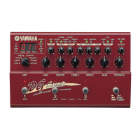
Detailed illustration and identification of controls on the top panel.

Foot Switch Section

Description of the foot switches used for operation.

Amplifier Section Controls

Detailed explanation of amplifier controls like Gain, Master, and Tone.

Effect Section Controls

Description of controls for modulation, delay, and reverb effects.

Rear Panel Connections

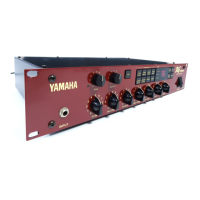
Identification of all rear panel input/output jacks and switches.

System Block Diagram

Disassembly Procedure

Bottom Case Removal

Steps for removing the bottom case of the unit.

DM Circuit Board Removal

Procedure for removing the main DM circuit board.

PN Circuit Board Removal

Steps for removing the PN 1/2 and PN 2/2 circuit boards.

LSI Pin Description

CPU LSI Pin Description

Detailed pin assignments and functions for the CPU LSI.

DSP6 LSI Pin Description

Pin assignments and functions for the DSP6 Digital Signal Processor.

Test Program Procedures

Starting the Test Program

Steps to initiate the diagnostic test sequence.

LED Check Procedure

Detailed steps for performing the LED diagnostic check.

Switch (SW) Check Procedure

Procedure for testing all switches and their indicators.

Control (VR) Check Procedure

Procedure for testing all variable resistors (controls).

DSP Electric Characteristic Test

Procedure for testing DSP electrical characteristics and output levels.

Troubleshooting Error Messages

Error E5: Backup Battery Error

Cause and solution for a depleted backup battery.

Parts List

Overall Assembly Diagram

Exploded view diagram of the unit's overall assembly.

Overall Circuit Diagram

Overall Circuit Diagram 1/2 (DM)

Schematic of the main digital processing section.

Overall Circuit Diagram 2/2 (PN Boards)

Schematic of the PN 1/2 and PN 2/2 circuit boards.

Related product manuals