RFSoC Data Converter Evaluation Tool User Guide 8
UG1287 (v2018.2) October 1, 2018 www.xilinx.com
Chapter 1: Introduction
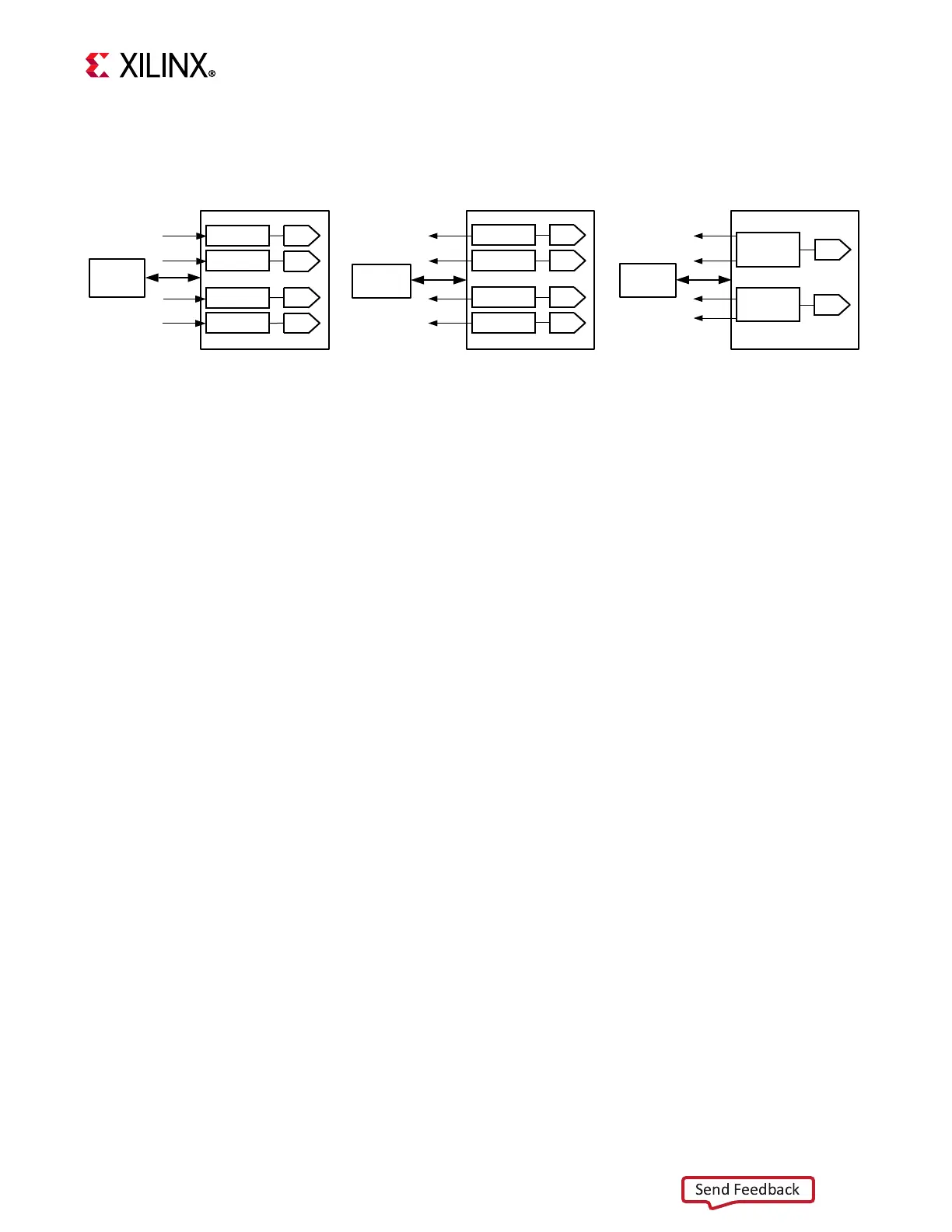
The RF-ADCs and RF-DACs are organized into tiles, each containing either two or four
RF-ADCs or four RF-DACs (see Figure 1-2). Each tile also includes a block with a PLL and all
the necessary clock handling logic and distribution routing for the analog and digital logic.
For device specifications and additional information, see:
• Zynq UltraScale+ RFSoC Data Sheet: Overview (DS889) [Ref 1]
• Zynq UltraScale+ RFSoC Data Sheet: DC and AC Switching Characteristics (DS926)
[Ref 2]
• Zynq UltraScale+ Device Technical Reference Manual (UG1085) [Ref 3].
X-Ref Target - Figure 1-2
Figure 1-2: Converter Tile Structure
DAC_X0Y0
Data Path 2
Data Path 3
Data Path 1
DAC1
Data Path 0
DAC0
IP State
Machine
s03_axis
s02_axis
s01_axis
s00_axis
6.4 GSPS RF-DAC Tile
ADC_X0Y1
Data Path 2
ADC2
Data Path 3
ADC3
Data Path 1
ADC1
Data Path 0
ADC0
m13_axis
m12_axis
m11_axis
m10_axis
2 GSPS RF-ADC Tile
ADC_X0Y0
Data Path 1
(23)
ADC1
(23)
Data Path 0
(01)
ADC0
(01)
m03_axis
m02_axis
m01_axis
m00_axis
4 GSPS RF-ADC Tile
IP State
Machine
IP State
Machine
DAC2
DAC3
X21300-090918
 Loading...