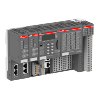
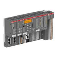
Table 13: Assignment of the terminals for PM5032-R-ETH and PM5052-R-ETH:
Terminal Signal Description
1 COM 0..11 Input common for digital input signals DI0 to DI11
2 I0 Digital input signal DI0 (5 kHz)
3 I1 Digital input signal DI1 (5 kHz)
4 I2 Digital input signal DI2 (5 kHz)
5 I3 Digital input signal DI3 (5 kHz)
6 I4 Digital input signal DI4 (100 kHz)
7 I5 Digital input signal DI5 (100 kHz)
8 I6 Digital input signal DI6 (100 kHz)
9 I7 Digital input signal DI7 (100 kHz)
10 I8 Digital input signal DI8
11 I9 Digital input signal DI9
12 I10 Digital input signal DI10
13 I11 Digital input signal DI11
14 NO0 Normally-open relay contact of the output NO0
15 NO1 Normally-open relay contact of the output NO1
16 NO2 Normally-open relay contact of the output NO2
17 R0..2 Output common for signals NO0 to NO2
18 NO3 Normally-open relay contact of the output NO3
19 NO4 Normally-open relay contact of the output NO4
20 NO5 Normally-open relay contact of the output NO5
21 R3..5 Output common for signals NO3 to NO5
22 C12 Digital input/output signal configurable DC12 (100 kHz,
if configured as output)
23 C13 Digital input/output signal configurable DC13 (100 kHz,
if configured as output)
24 UP Process supply voltage UP +24 V DC
25 ZP Process supply voltage ZP 0 V DC
The following block diagram shows the internal structure of the onboard I/Os.
Block diagrams
Processor modules > PM50xx
2021/06/29 3ADR010635, 2, en_US 81
 Loading...