Do you have a question about the ADLINK Technology arm AMPERE COM-HPC-ALT and is the answer not in the manual?
Provides legal and liability information regarding the use of ADLINK products and intellectual property.
Details ADLINK's commitment to environmental preservation and compliance with RoHS and WEEE directives.
Lists product names used for identification purposes and acknowledges registered trademarks.
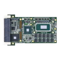
Details the system-on-chip (SoC) options and their core counts, clock speeds, and TDP.
Outlines the various expansion bus interfaces like PCIe, their configurations, and speeds.
Details the Ethernet interfaces, including NBASE-T and KR/KX types, and their capabilities.
Covers various input/output interfaces like USB, UART, and GPIO, including their configurations.
Describes additional features such as FAN control and health monitoring, including voltage and temperature monitoring.
Details security-related hardware components like the Trusted Platform Module (TPM).
Explains the function and connectivity of the Module Management Controller (MMC) for system management.
Describes the debug connector and its uses for carrier design and module bring-up.
Details the power modes, input voltage requirements, and power management states supported by the module.
Specifies the module's physical dimensions, operating temperature, humidity, and environmental testing standards.
Provides a comprehensive list of all signal pins on the COM-HPC connectors (J1 and J2).
Defines terms used in signal description tables for clarity and understanding of pin functions.
Details the specific signal assignments for various interfaces like Ethernet, USB, PCIe, I2C, and SPI on the J1 and J2 connectors.
Describes the 40-pin debug connector and its critical access points for carrier design.
Identifies and explains the function of the status LEDs (LED1, LED2, LED3) on the module.
Details the fan connector type and its pin assignments for fan control.
Provides step-by-step instructions for performing a hardware reset of BIOS default settings.
Explains how to configure BIOS boot modes (PICMG vs. Failsafe) using switches.
Lists and describes the status code ranges used for diagnosing boot process issues.
Shows the physical dimensions of the COM-HPC module in millimeters.
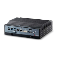
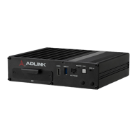
Presents different thermal solutions available for the module, including heatsinks and coolers.
| Form Factor | COM-HPC |
|---|---|
| Processor | Ampere Altra |
| Architecture | Arm |
| CPU Cores | Up to 80 cores |
| Memory | Up to 1 TB DDR4 |
| Ethernet | Up to 2x 10GbE |
| Storage | NVMe |
| Expansion | PCIe Gen4 |
| USB | USB 3.0, USB 2.0 |
| PCIe | Up to 64 PCIe Gen4 lanes |
| Power Consumption/TDP | Up to 175W |
| Operating Temperature | 0°C to +60°C |