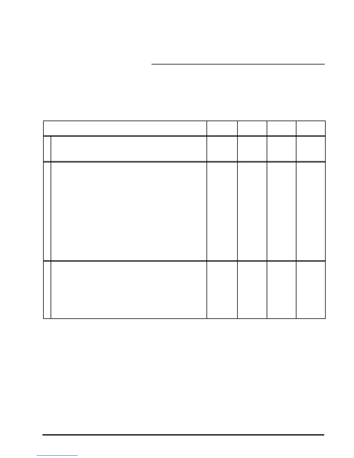
Dielectric etch
Stripping
Resist and polyamid etch
Metal etch (Al, W, Ta, Ti, TiN)
Polysilicon etch
Ion implant (source)
Tungsten CVD (W CVD)
Titanium and Titanium nitride CVD (Ti, TiN CVD)
Silicon epitaxy
SiO
2
CVD using silane as silicon source
Polysilicon CVD
Undoped SiO
2
HDPCVD
IPUP
A100P
13000h
(1.5 years)
13000h
(1.5 years)
26000 h
(3 years)
HARSH
Non doped SiO
2
CVD using TEOS
Doped SiO
2
CVD using TEOS (PSG, BSG, BPSG)
SACVD oxide using TEOS
Silicon nitride and nitroxide PECVD
Silicon nitride LPCVD
MOCVD doped using phosphorus
Doped SiO
2
CVD using phosphorus, boron or fluorine HDPCVD
IPUP
A100P
/ / 8500 h
(1 year)
Maintenance times can change according to processes and equipment used.