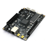
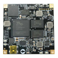
ARTIX-7 FPGA Development Board AX7101 User Manual
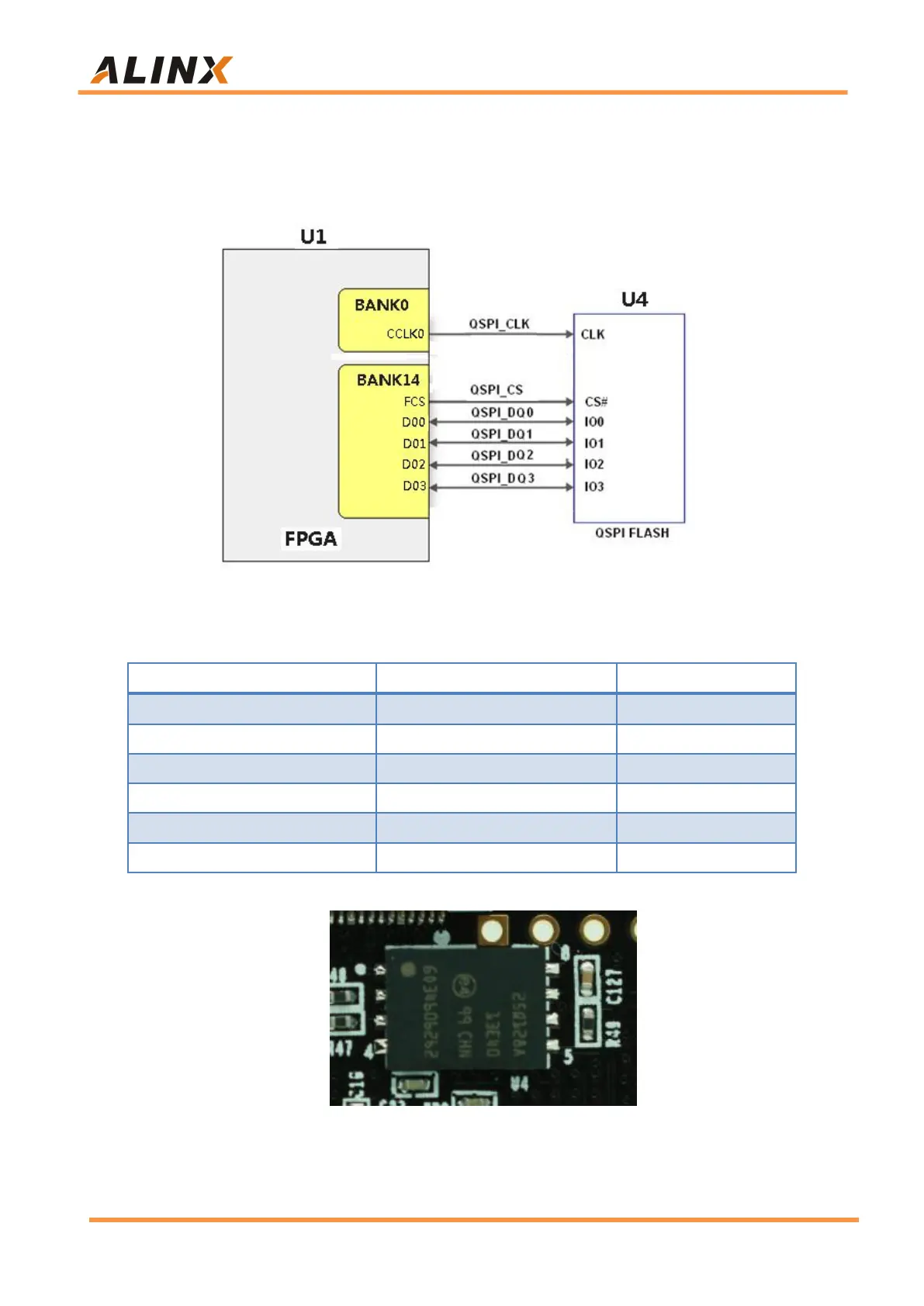
the FPGA chip. The clock pin is connected to CCLK0 of BANK0, and other data
and chip select signals are connected to D00~D03 and FCS pins of BANK14
respectively. Figure 2-5-1 shows the hardware connection of QSPI Flash.
Figure 2-5-1: QSPI Flash Schematic
QSPI Flash pin assignments:
Figure 2-5-2: QSPI on the Core Board


 To Next Page