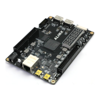
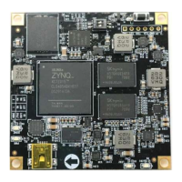
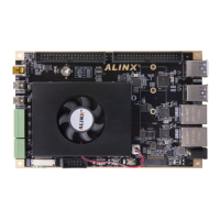
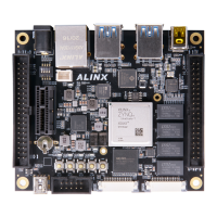
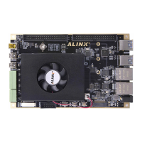
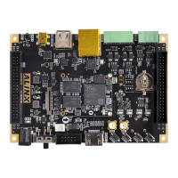
ARTIX-7 FPGA Development Board AX7101 User Manual
following table:
FPGA auxiliary voltage, TPS74801 power supply
VCCIO of Bank0,Bank13 and Bank14 of FPGA,QSIP FLASH, Clock Crystal
DDR3, Bank34 and Bank35 of FPGA
GTP Transceiver Bank216 of FPGA
GTP Transceiver Bank216 of FPGA
Because the power supply of Artix-7 FPGA has the power-on sequence
requirement, in the circuit design, we have designed according to the power
requirements of the chip, and the power-on is 1.0V->1.8V->(1.5 V, 3.3V, VCCIO)
and 1.0V-> MGTAVCC -> MGTAVTT, the circuit design to ensure the normal
operation of the chip.
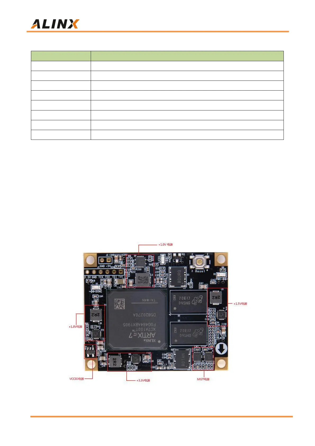
The power circuit on the AC7100B FPGA core board is shown in Figure
2-11-2:
Figure 2-11-2: Power Supply on the AC7100B FPGA Core Board


 To Next Page