KINTEX UltraScale+ FPGA Board AXKU040 User Manual
Part 4: QSPI Flash
The AXKU040 FPGA development board is equipped with one 128MBit
Quad-SPI FLASH, and the model is N25Q128A, which uses the 3.3V CMOS
voltage standard. Due to the non-volatile nature of QSPI FLASH, it can store
FPGA configuration Bin files and other user data files in use. The specific
models and related parameters of QSPI FLASH are shown in Table 4-1.
Table 4-1: QSPI FLASH Specification
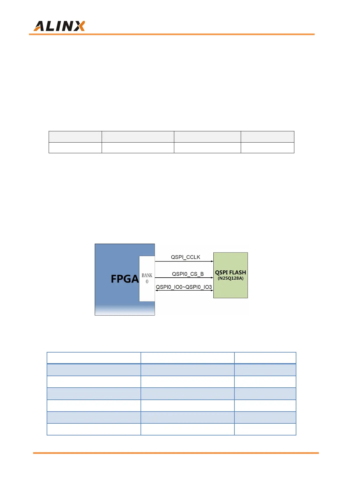
QSPI FLASH is connected to the dedicated pins of BANK0 of the FPGA
chip. The clock pin is connected to CCLK0 of BANK0, and other data signals
are connected to D00~D03 and FCS pins. Figure 4-2 shows the hardware
connection of QSPI Flash and FPGA Chip.
Figure 4-2: QSPI Flash Schematic
QSPI Flash pin assignments: