KINTEX UltraScale+ FPGA Board AXKU040 User Manual
Part 16: Keys
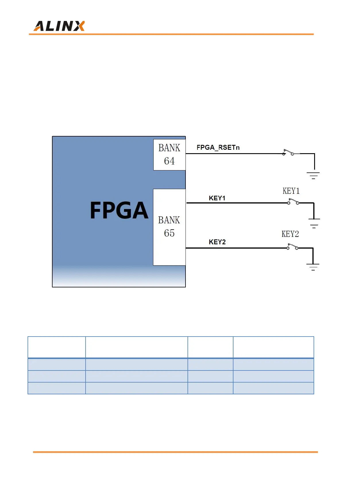
The AXKU040 FPGA development board contains two user Keys and 1
reset key. Two user keys are connected to the IO of FPGA BANK65.The user
key is active at low level to realize some functions of the board for customers;
The reset key is connected to FPGA BANK64 for system reset.
The circuit of user key part is shown in Figure 16-1.
Figure 16-1: Keys Schematic
Keys Pin Assignment
IO_L24P_T3U_N10_EMCCLK_65