KINTEX UltraScale+ FPGA Board AXKU040 User Manual
Part 5: Clock configuration
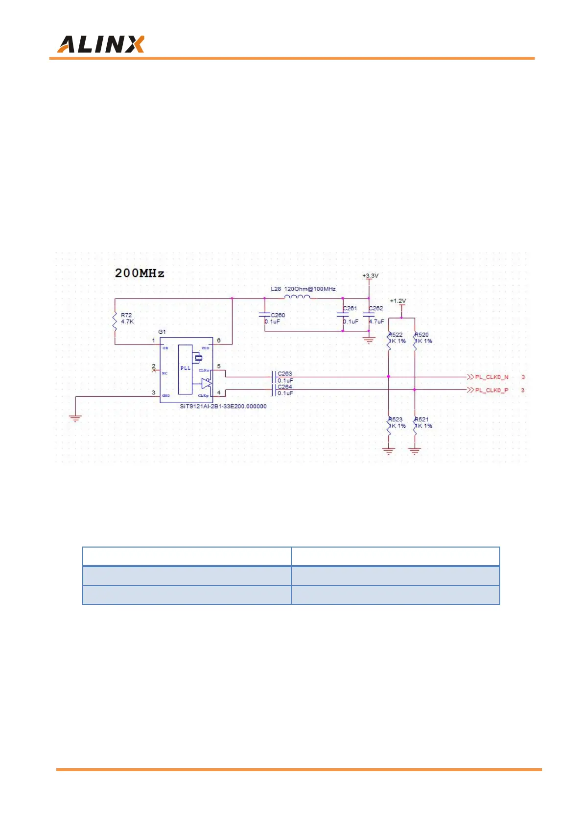
Part 5.1: 200Mhz differential clock source
A differential 200MHz clock source is provided on the FPGA development
board to provide the system clock to the FPGA. The crystal differential output is
connected to the FPGA BANK45, which can be used to drive the DDR
controller operating clock and other user logic in the FPGA. The schematic
diagram of the clock source is shown in Figure 5-1.
Figure 5-1: 200Mhz System Clock Source Schematic
System Clock pin assignments:
Part 5.2: 125Mhz differential clock source
A differential 125MHz clock source is provided on the FPGA development
board to provide the clock for transceiver GTH. The crystal differential output is
connected to the FPGA BANK224, which can be used for the clock required by
4 optical fibers. The schematic diagram of the clock source is shown in Figure