KINTEX UltraScale+ FPGA Board AXKU040 User Manual
Part 17: Power Supply
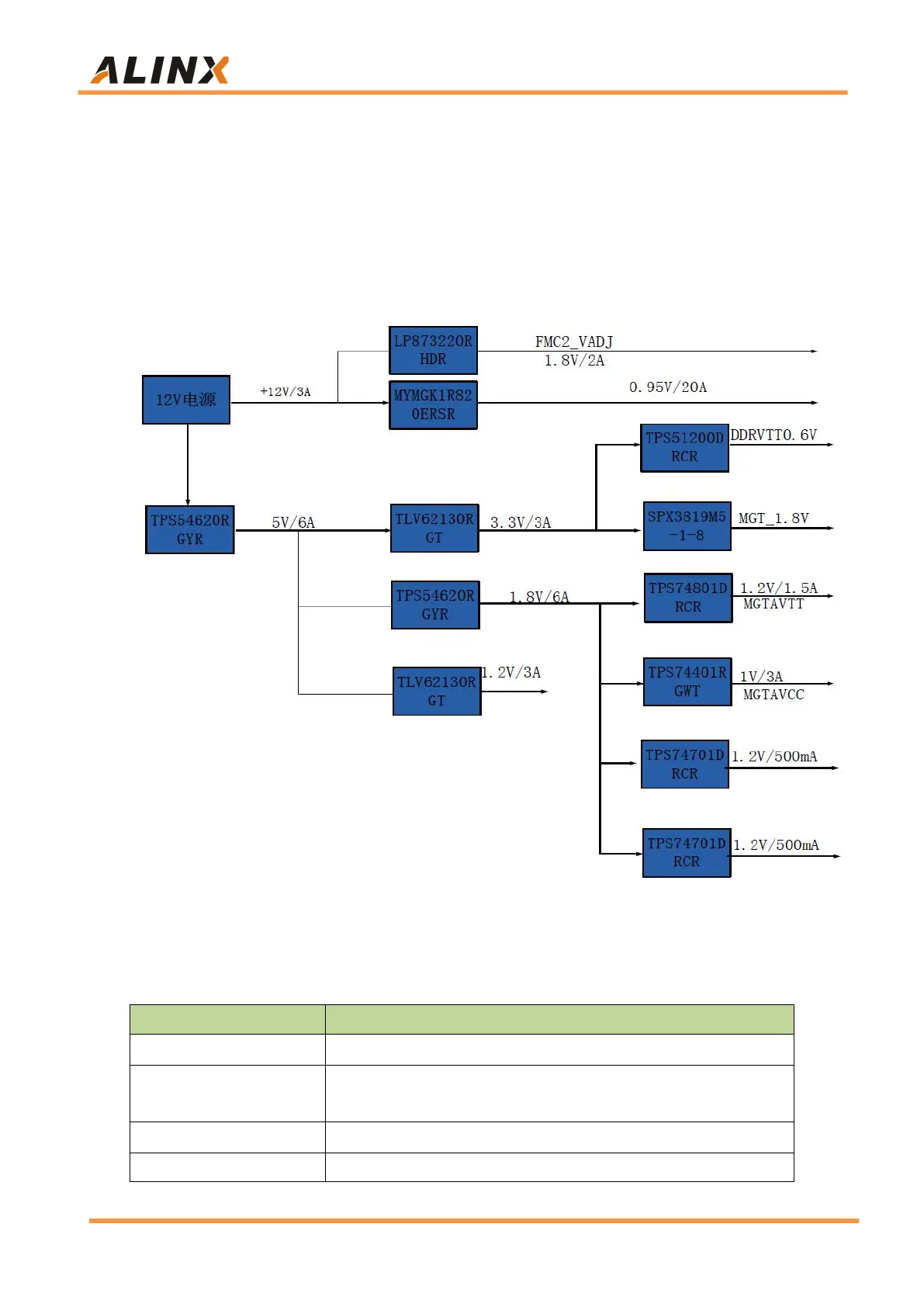
The power input voltage of the AXKU040 FPGA development board is
DC12V, and the external +12V power supply supplies power to the FPGA
development board.
The Power supply design diagram shown in Figure 18-1.
Figure 17-1: Power Supply Design Diagram
The functions of each power distribution are shown in the following table:
FMC Chip IO Voltage, FMC, SFP, LED, SD Card, Level
Conversion Chip
HDMI Chip, Level Conversion Chip, Power Supply Voltage
DDR4, FPGA Chip, Voltage in the FMC