KINTEX UltraScale+ FPGA Board AXKU040 User Manual
5-2.
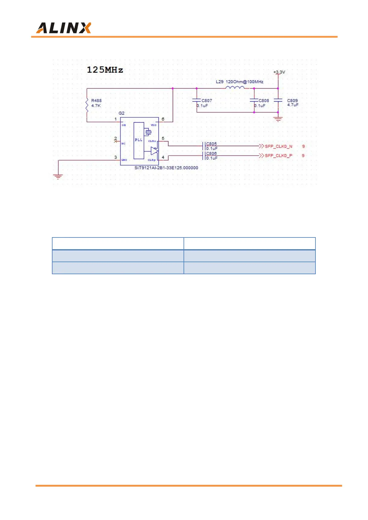
Figure 5-2: 125Mhz System Clock Source Schematic
System Clock pin assignments:
Part 5.3: 156.25Mhz differential clock source
A differential 156.25MHz clock source is provided on the FPGA
development board to provide the clock to the FPGA Transceiver GTH. The
crystal differential output is connected to the FPGA BANK228. The schematic
diagram of the clock source is shown in Figure 5-3.