KINTEX UltraScale+ FPGA Board AXKU040 User Manual
Part 12: SMA and SATA Interface
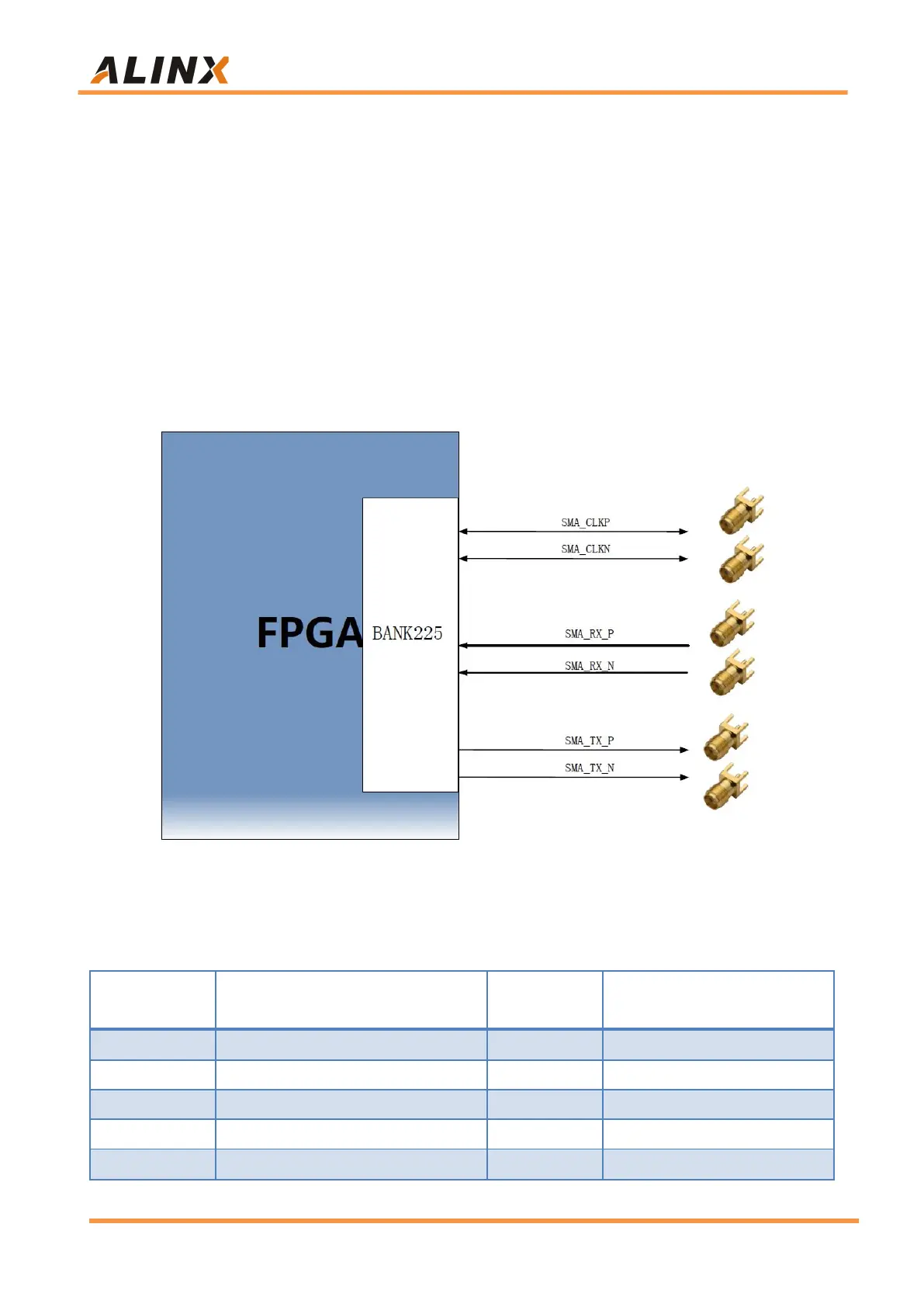
The AXKU040 FPGA development board is designed with 6 SMA
interfaces, which are connected to the BANK225 high-speed transceiver ,
including a pair of TX, a pair of RX, and a pair of clock signals. Provide
customers with high-speed external interfaces. In addition, two SATA ports are
reserved on the FPGA board for connecting solid state drives.
The schematic diagram of FPGA and SMA interface connection is shown
in Figure 12-1.
Figure 12-1: SMA Connection Schematic
SMA Interface pin assignment:
Transceiver Signal Output
Transceiver Signal Output