KINTEX UltraScale+ FPGA Board AXKU040 User Manual
Part 8: HDMI Video Output Interface
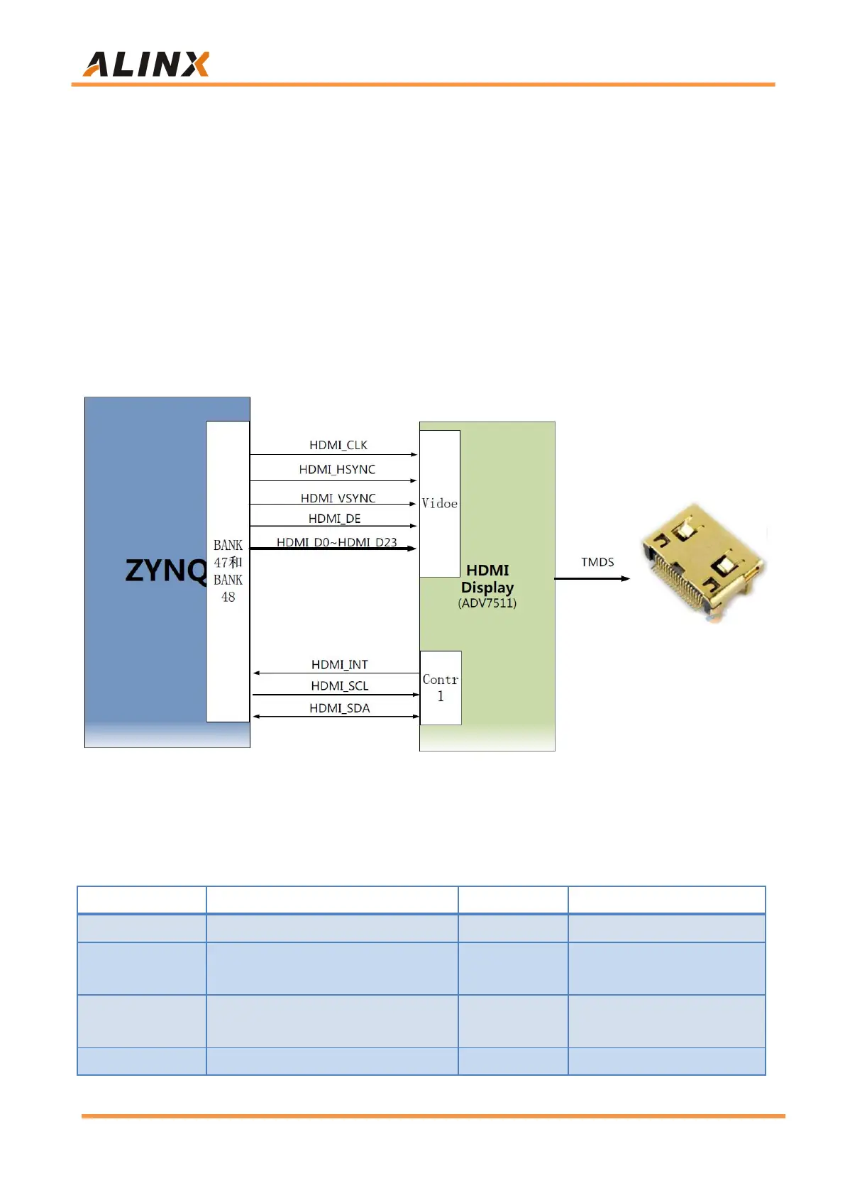
The HDMI output interface uses the ADV7511 HDMI (DVI) encoding chip
from ANALOG DEVICE, which supports up to 1080P@60Hz output and 3D
output.
The video digital interface, audio digital interface and I2C configuration
interface of ADV7511 are connected to the IO of BANK47 and BANK48.
The hardware connection diagram of ADV7511 chip and XCKU040 is
shown in Figure 8-1:
Figure 8-1: HDMI Output Interface Schematic
ADV7511 pin assignment:
HDMI Video Signal Line
Synchronization
HDMI Video Signal Column
Synchronization