KINTEX UltraScale+ FPGA Board AXKU040 User Manual
FPGA power supply system
XCKU040 FPGA power supplies are VCCINT, VCCBRAM, VCCAUX, VCCAUX_IO VCCO,
VMGTAVCC , VMGTAVTT, VMGTVCCAUK , VMGTAVTTRCAL, VCCADC. VCCINT is the FPGA core power
supply pin, which needs to be connected to 0.95V; VCCBRAM is the power supply
pin of FPGA Block RAM, connect to 0.95V; V
CCAUX
and V
CCAUX_IO
are FPGA
auxiliary power supply pin, connect 1.8V; VCCO is the voltage of each BANK of
FPGA, including BANK0, BANK44~48, BANK64~68. VMGTAVCC is the power
supply voltage of the GTH and GTY transceivers inside the FPGA, connected
to 1.0V; V
MGTAVTT
is the terminal voltage of GTH transmission and reception,
connected to 1.2V. VMGTAVTTRCAL is the transceiver resistance calibration voltage,
connect to 1.2V. VCCADC is the supply voltage of XADC, connected to 1.8V.
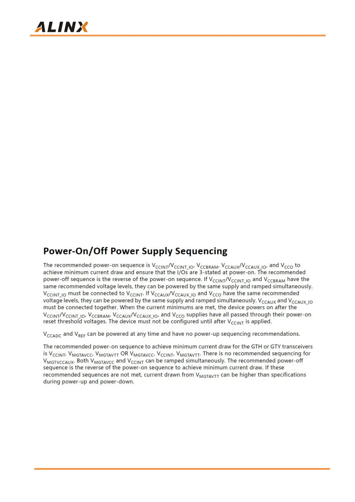
The XCKU040 FPGA system requires the power-on sequence as shown in
Figure 2-2.
Figure 2-2: Power-On/Off Power Supply Sequencing