Preliminary Technical Data UG-1828
Rev. PrC | Page 233 of 338
Figure 215. Differential Receiver Interface Using a Transmission Line Balun
Given wide RF bandwidth applications, SMD balun devices function well offering acceptable differential balance and insertion loss in a
relatively small (0603, 0805) package.
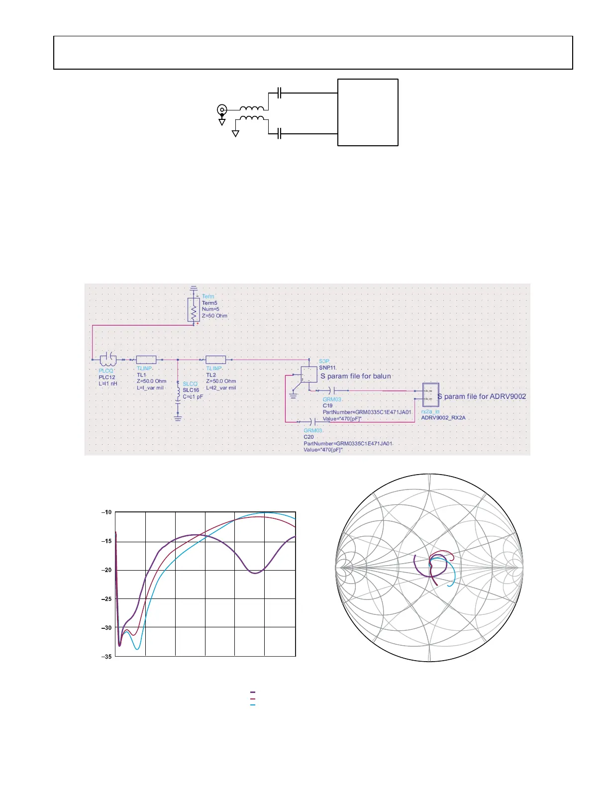
Example of RX1 A Port Frequency Match Simulation
Reasonable approximation of return loss of a frequency matching network can be obtained with a simple S parameter simulation available
in ADS without PCB artwork. Figure 216 illustrates a wide-band frequency match simulation setup in ADS for ADRV9001 RX1(2) A
input pins in ADS for evaluating a possible configuration for a desired match to 3 GHz.
Figure 216. ADS Simulation Example Setup with Simple Physical Board Trace Models
Figure 217. ADS Simulation Results of Return Loss Curve
Rx1A/1B/2A/2B –
Rx1A/1B/2A/2B+
RECEIVER
INPUT
STAGE
C
C
C
C
24159-165
AT THE FINAL SERIES INDUCTOR WITH A SHORT TL
AT THE SINGLE-ENDED TERMINAL OF BALUN
AT THE FIRST SHUNT CAPACITOR WITH A SHORT TL
S (5,5) (H)
FREQUENCY (10MHZ TO 3GHZ)
dB (S(5,5)) (H)
FREQUENCY (GHz)
H
0 0.5 1.0 1.5 2.0 2.5 3.0
24159-167
 Loading...