UG-1828 Preliminary Technical Data
Rev. PrC | Page 248 of 338
Table 102. Device Clock Input Interface Modes Description
Voltage Applied at
MODEA Pin
Device Clock Input
Electrical Interface
DEV_CLK_OUT Divider Value Applied
to DEV_CLK_IN Signal Note
0 V (grounded) LVDS /16 Up to 1GHz clock
0.45 V CMOS or XTAL /2 CM0S(10MHz to 80MHz)
/XTAL(20 MHz to 80 MHz) with
Nominal Gm multiplier = x8
0.9 V CMOS or XTAL /2 CM0S(10MHz to 80MHz)
/XTAL(20 MHz to 80 MHz) with
Nominal Gm multiplier = x6
1.35 V CMOS or XTAL /2 CM0S(10MHz to 80MHz)
/XTAL(20 MHz to 80 MHz) with
Nominal Gm multiplier = x2
1.8 V CMOS or XTAL /2 CM0S(10MHz to 80MHz)
/XTAL(20 MHz to 80 MHz) with
Nominal Gm multiplier = x4
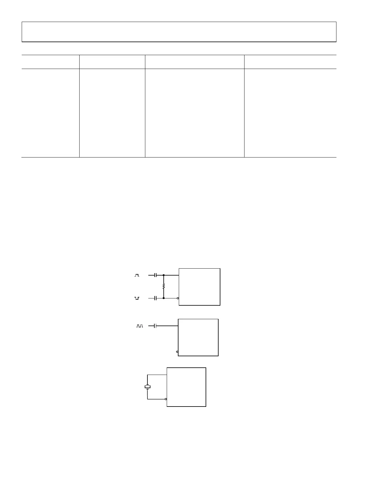
By applying 1.8 V to MODEA pin A for CMOS interface mode, a clipped sinewave clock signal from a TCXO can be applied to pin
named DEV_CLK_IN+(E7) via a AC coupling capacitor and pin DEV_CLK_IN-(E8) should be left unconnected as shown in Figure 237.
A Xtal should be connected to both DEV_CLK_IN+ and DEV_CLK_IN- pins with a DC voltage between 0.45 and 1.8 V applied to
MODEA pin as shown in Figure 238.
When LVDS mode input clock interface is selected with MODEA pin grounded, an external clock is used as the reference clock for the
RFPLL and the Clocking PLL on the device and thus must be a very clean clock source. Connect the external clock inputs to the
DEV_CLK_IN+ (E7) and DEV_CLK_IN- (E8) balls via AC coupling capacitors and should be terminated with 100 Ω as shown in
Figure 236. The inputs are biased on the device to a 200 mV voltage level. The input impedance plot over operating frequency is shown on
Figure 216. The operational frequency range of the DEV_CLK signal is between 10 MHz and 1000 MHz. Ensure that the external clock peak-
to-peak amplitude does not exceed 800mV (Note that either positive and negative side of differential input pins should not exceed 400mV
peak-to-peak.). For best synthesizer performance, a high slew rate signal is best with fast rise and fall times.
Device Clock Interface Modes
Figure 236. LVDS Interface Mode
Figure 237. CMOS Interface Mode
Figure 238. Crystal (XTAL) Interface Mode
DEV_CLK_IN+
LVDS
CLOCK
100nF
100Ω
E8
E7
100nF
DEV_CLK_IN–
24159-186
DEV_CLK_IN+
CMOS
CLOCK
100nF
E8
E7
UNCONNECTED
DEV_CLK_IN–
24159-187
DEV_CLK_IN+
E8
E7
DEV_CLK_IN–
24159-188
 Loading...