Preliminary Technical Data UG-1828
Rev. PrC | Page 255 of 338
• Differential lines from the balun to the Rx and Tx pins must be as short as possible. The length of the single ended transmission line
should also be short to minimize the effects of parasitic coupling.
• The system designer can optimize the RF performance with the proper selection of balun, matching components, and ac coupling
capacitors. The external LO traces and the DEV_CLK_IN traces may require matching components as well to ensure optimal
performance. Matching network design is explained in greater detail in the RF Port Interface Information section of this document.
• RF signal path isolation is critical to achieving the level of isolation specified in the ADRV9001 datasheet. More details on proper
isolation are provided in the Isolation Techniques Used on the ADRV9001 Evaluation Card section.
• For each RF Tx output, install a 10µF capacitor near the balun power supply pin connected to the VANA1_1P8, VANA2_1P8
supplies. If baluns with no dc supply connection are used, power will must be supplied to the Tx outputs using RF chokes. Connect
chokes between the VANA1_1P8 and Tx1 output and VANA2_1P8 and Tx2 output respectively. In both cases, the 10µF capacitor
acts as a reservoir for Tx supply current. The TX Balun DC Supply Options section describes the Tx output power supply
configuration in more detail.
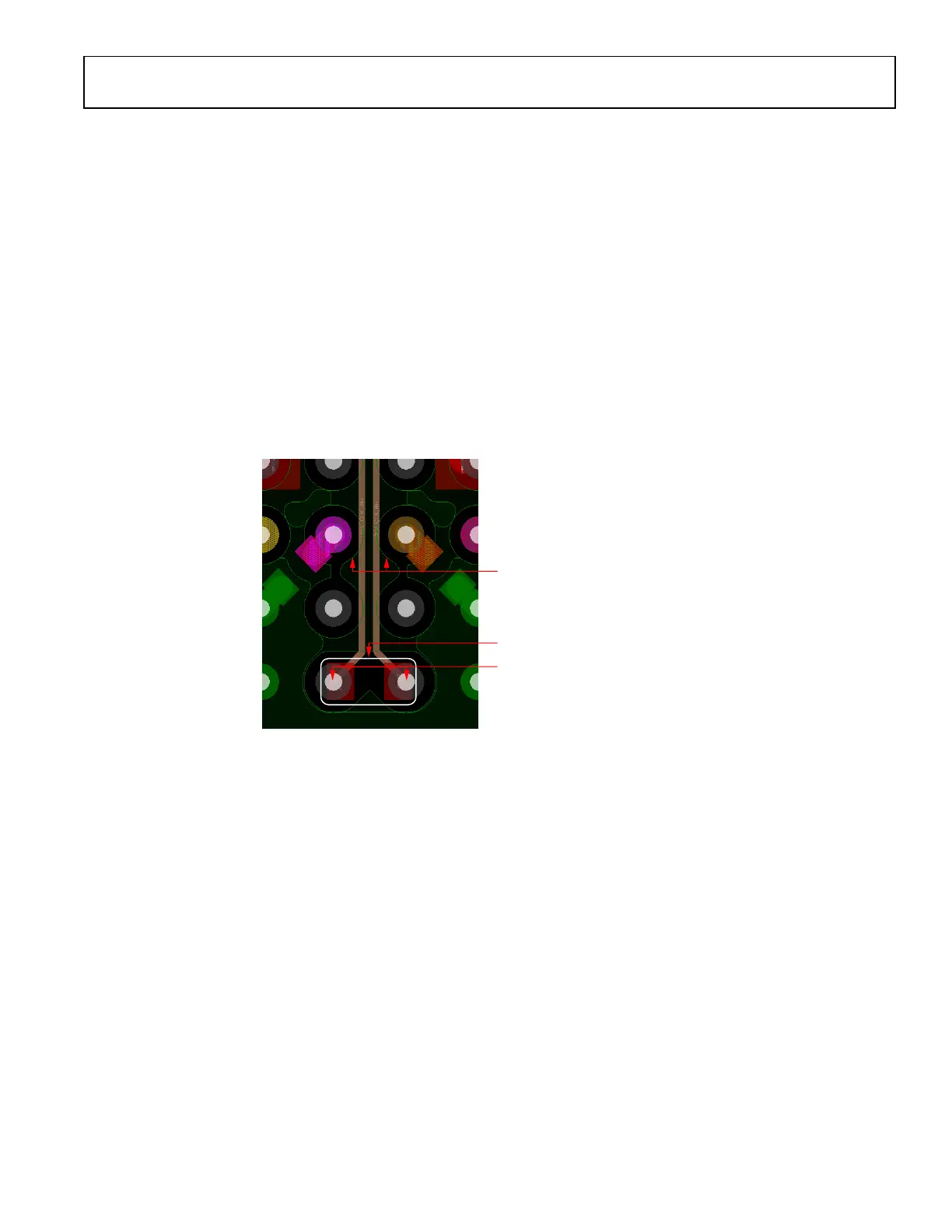
• Connect the external clock inputs to the DEV_CLK_IN+ (E7) and DEV_CLK_IN− (E8) pins using ac coupling capacitors. Use a
100 Ω termination at the input to the device. Figure 243 illustrates the recommended placement for termination resistor near the
DEV_CLK_IN pins. Traces should be shielded by surrounding ground with vias staggered along the edge of the differential trace
pair. This arrangement creates a shielded channel that prevents the reference clock from any interference from other signals. Refer to
the ADRV9001 evaluation card layout for exact details.
Figure 243. DEV_CLK_IN Signal Routing Recommendations
• The EXT_LO1+ (A12), EXT_LO1- (A11), EXT_LO2+ (A3), EXT_LO2- (A4) pins are internally dc biased. If an external LO is used,
connect it via ac coupling capacitors.
• The data port interface should be routed at the beginning of the PCB design and with the same priority as RF signals. This is
especially important if data port runs in LVDS configuration. Attention should be paid to provide appropriate isolation between data
port differential pairs.
Signals with Secondary Routing Priority
Power supply quality has direct impact on overall system performance. To achieve optimal performance, users should follow
recommendations regarding power supply routing. The following recommendations outline how different power domains should be
routed and which supplies can be tied to the same supply but separated by a ferrite bead.
A general recommendation for power supply routing is to follow the star methodology in which each power domain is deliver by a
separate trace from the source supply. Care should be taken to make sure that each power trace is surrounded by ground. Figure 244
shows an example of such traces routed on the evaluation card on layer 3. Each trace is separated from any other signal by ground plane
fill and vias. This approach is essential to providing necessary isolation between power domains.
BGA BALLS
100Ω TERMINATION
RESISTOR
DEV_CLK_IN
TRACES (INNER LAYER)
24159-192
 Loading...