UG-1828 Preliminary Technical Data
Rev. PrC | Page 274 of 338
Figure 261 provides simulation schematic with power supply filter components used on EVB power rails in ADS environment. It basically
attempts to simulate frequency response of filter outlined in Figure 260.
• The E1, C1, E2, and C2 elements be located right at each rail input pin.
• The E3, and C4 elements be located right at trace that feeds particular pin.
• The C4 element is the RF capacitor that should be placed right at each ADRV9001 pin using the rail. For more information
about placing of those capacitors refer to PCB layout section and EVB PCB file itself.
• The combined DC resistance of the three ferrites is 0.106Ω.
Figure 261. ADS model of C/FB/C/FB cascaded filter utilized on ADRV9001 EVBs
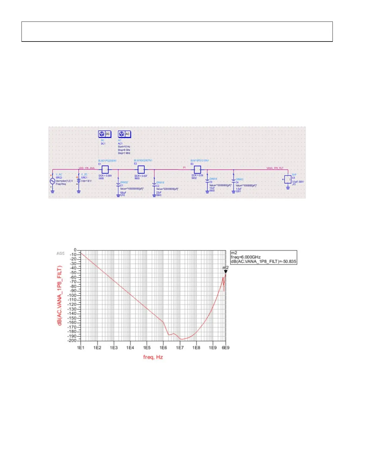
Finally Figure 262 provides results of simulation that is described in Figure 261. The overall frequency response is better than typical bank
of capacitor. The region >1 GHz outlines performance of implemented cascaded C/FB/C/FB filtering approach.
Figure 262. Response of C/FB/C/FB cascaded filter utilized on ADRV9001 EVBs
Care must be taken when introducing multiple inductors and ferrite beads in series creates issue with potential IxR voltage drop on them
that could violate recommended power domain voltage accuracy. Power supply solution on ADRV9001 EVB uses sense line to monitor
the voltage output after the ferrite bead (where possible). This approach ensures that the voltage drop resulting from the cascaded filters
and FB resistance is taken into account and the voltage level delivered to the ADRV9001 is in line with expected accuracy. In scenarios
where single power domain powers multiple power pins, current tends to be distributed over multiple pins and this helps with
minimizing IxR voltage drop on FB components.
 Loading...